AN-CM-296 Smart Lock Motor Driver with Voltage Regulation
Renesas Electronics CorporationThis application note describes GreenPAK, configured as a Brushed DC motor driver with constant voltage regulation and motor on/offcontrol by current sensing.
AN-CM-339 Ultrasonic Humidifier
Renesas Electronics CorporationThis application note describes how to implement an ultrasonic humidifier with some additional features.
AN4892: RTG4 SRAM Initialization After Powerup Using μPROM Application Note (AC454)
Microchip Technology Inc.This application note describes how to initialise the Static Random Access Memory (SRAM) blocks of Microchip RTG4 Field Programmable Gate Array (FPGA) with user data after power-up. The design for this application note uses a Large SRAM (LSRAM) block, which is initialised by an FPGA fabric master through the Advanced Microcontroller Bus Architecture Advanced Peripheral Bus interface (AMBA APB bus).
RTG4 FPGA devices have embedded SRAM blocks (LSRAM and µSRAM) in the fabric. Both LSRAM and µSRAM blocks are placed in multiple rows within the FPGA fabric, and they can be accessed through the fabric routing architecture.
.jpg)
ANP114 - Voltage and Frequency Dependence of Ferroelectric Class 2 Multilayer Ceramic Capacitors
Wurth ElektronikFerroelectric multilayer ceramic capacitors (MLCCs) are electronic devices that exhibit the property of ferroelectricity, which means they can maintain stable electric polarization even in the absence of an external electric field and therefore have a voltage-dependent capacitance. Würth Elektronik has implemented the voltage capacitance behavior in the LTSpice files. The underlying model development is explained in this appnote. The use of the MLCC, e.g. for filtering, is thus significantly simplified for the developer. MLCCs are widely used in various electronic devices for energy storage and filtering.
This application note explains the voltage and frequency dependence of ferroelectric MLCCs. After an introduction to ferroelectricity, a mathematical model for the capacitance-voltage behavior of ceramic MLCCs is derived from a dipole polarization model. The parameters of the model are reduced to two fitting parameters. To demonstrate the practical applicability, the model is tested by measurements on a selection of MLCCs from Würth Elektronik's portfolio. Since the integral of the capacitance-voltage model mathematically contains only basic trigonometric expressions, it can be easily implemented in software that requires functions of charge instead of capacitance, such as the simulation software Spice. Furthermore, it is shown that the model can be used to describe the capacitance spectra of MLCCs at different DC voltages.
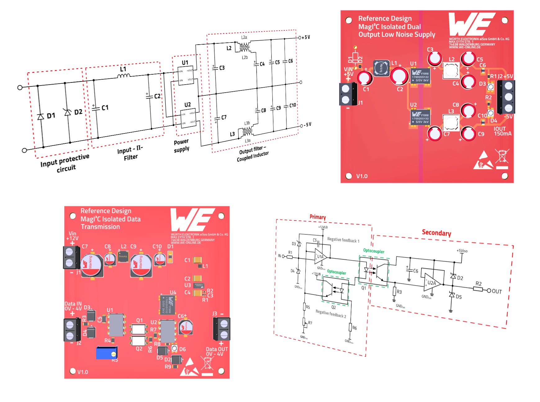
ANS019 - Bipolar power supply and isolated signal transmission with MagI³C-FIMM
Wurth ElektronikIndustrial plants, such as warehouse logistics, filling plants, rolling mills, conveyor belts and printing presses, generally require the use of a selection of the following elements for safe operation:
- Isolation amplifiers, analog-to-digital converters
- Isolation of digital circuits
- Interfaces/bus isolation - RS232, RS485, CAN, Interbus, Profibus
- Measurement and data acquisition
All these applications have one thing in common, namely the isolation of the input supply voltage from the supplying bus voltage. But why galvanically isolate a supply from a bus or from switching components in general? Galvanic isolation prevents transient interference from the supply voltage from propagating into the bus and disrupting its operation.
All these applications share the fact that they are supplied by a power module with galvanic isolation. The Application Note explains the functionality and structure of the power module used for the applications described.
AN-CM-328 16-bit Sigma-Delta ADC
Renesas Electronics CorporationThis application note describes the implementation and testing of a 16-bit sigma-delta analog-todigital converter (ADC) based on the SLG47004 IC. The design requires few internal analog and digital resources, so the ADC can be integrated with other projects inside one SLG47004.
AN-CM-326 Analog Front-End for Electrocardiogram Monitor
Renesas Electronics CorporationThis application note describes the design of an analog front-end for an electrocardiography device. The circuit utilises the commonly used technique of measuring electrical heart activity using three electrodes applied to the arms and legs. These electrodes detect the small electrical signal that results from cardiac muscle contraction (the heartbeat). The unique auto-trim feature of the SLG47004 enables output signal level stabilization in conditions of interference and baseline drift. The application note also contains test results of a hardware prototype.
AN-CM-324 Adjustable Analog Sine - Square Wave Oscillator
Renesas Electronics CorporationThis application note describes how to design and build an adjustable, encoder-controlled, two-range sine / square wave oscillator using the SLG47004 IC.
AN-CM-303 8-bit SISO, SIPO, PISO, PIPO Shift Registers
Renesas Electronics CorporationThis application note shows how to implement various 8-bit shift registers within the GreenPAK IC. Serial in serial out, Serial in parallel out, Parallel in serial out, and Parallel in parallel out shift registers have been designed in the examples.
AN-CM-307 Analog Front End for Heart Rate Monitor
Renesas Electronics CorporationThis application note illustrates how to use the SLG47004 to implement an adjustable analog filter and describes different ways to adjust the filter`s cutoff frequency.
AN-CM-366 Automatic Voltage Switch Using SLG59H1008V
Renesas Electronics CorporationPortable electronic device or cordless devices are becoming ubiquitous in recent years thanks to the advantages they bring to the table in terms of size mobility and flexibility in their deployment. For starters, the numerous problems arise with the need to manage different voltage rating switched power supplies in order to maintain charge all devices. Practically it’s possible to connect a wrong power supply and eventually damage the device, sometimes beyond repair. There is a solution to solve this kind of problems which can enable multiple devices operating at different voltage levels to share the same power supply without a problem as long the voltage range is supported and if not, it will prevent the wrong voltage from passing through. To achieve this, a High Voltage GreenFET technology device is required to perform within the selected voltage range, over voltage and under voltage protection, and MCU to automate the process.
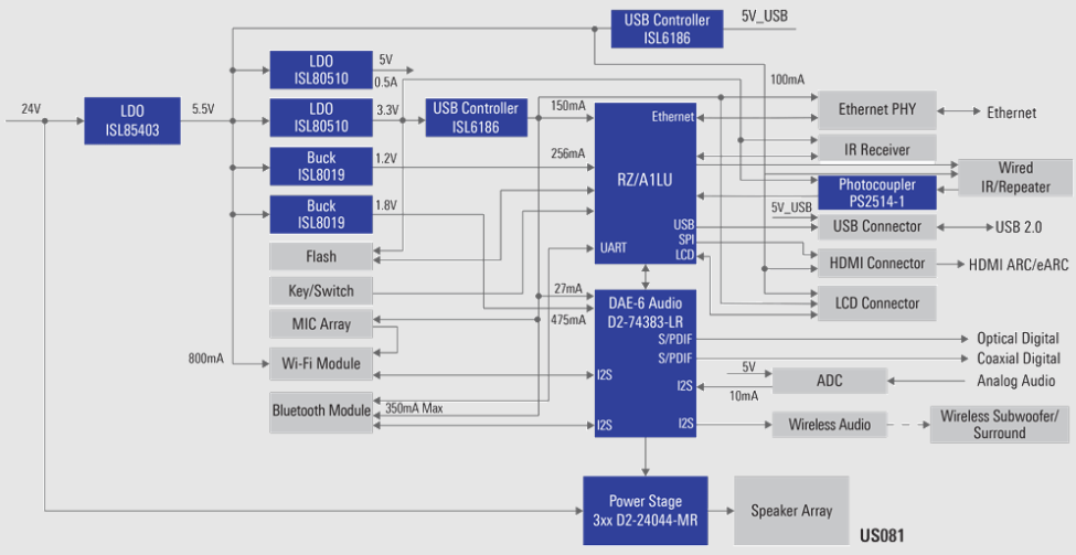
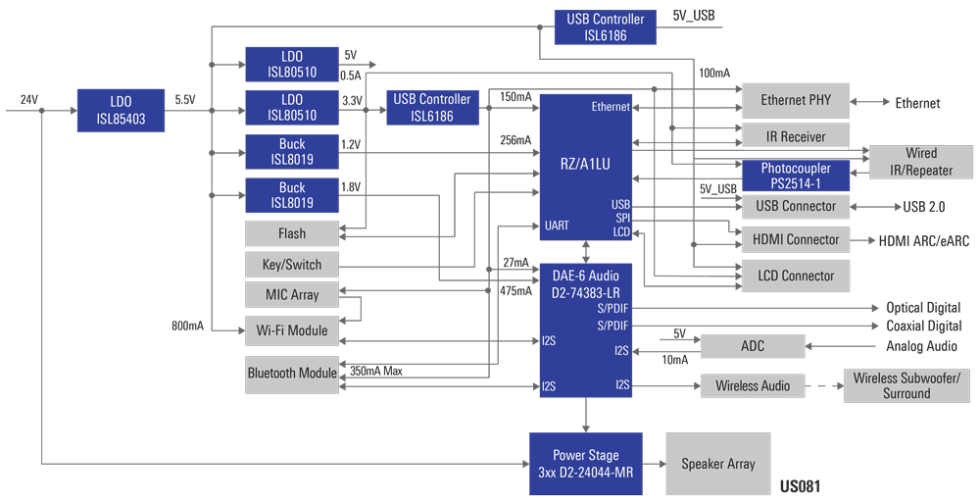
Alexa Controlled Soundbar
Renesas Electronics CorporationThe rising popularity of global on-demand streaming services has allowed consumers to enjoy content on various devices, challenging the traditional dominance of televisions. Alongside this, the world has seen an increase in the soundbar market. Recognising this trend, Renesas has introduced this to enable designers to create next-generation soundbars.
System Benefits:
- Complete soundbar design: Left and Right surround sound with subwoofer. Bluetooth and Wi-Fi (with "Alexa" voice control) inputs. Coaxial and optical SPDIF with 7ch output.
- The D2-6 family of intelligent digital audio processor devices are complete System-on-Chip (SoC) audio processor and Class-D amplifier controllers.
- The Cost-effective RZ/A1 MPU device with an Arm® Cortex®-A9 core running at 400MHz and 3MB of on-chip SRAM.
- The D2-24044 audio integrated power stage device is a high-performance, integrated Class-D amplifier power stage.
.png)
AN-2554: Step Counting Using the ADXL367
Analog Devices Inc.This application note describes the implementation of a pedometer algorithm for the ADXL367, a 3-axis digital accelerometer. The algorithm is based on peak detection analysis of the acceleration produced by a step over a predefined time window. Empirical results for a wrist worn use case show approximately 97% average accuracy under different scenarios.
AN-617: Wafer Level Chip Scale Package (WLCSP)
Analog Devices Inc.The Wafer Level Chip Scale Package (WLCSP) represents a cutting-edge variant of the flip-chip interconnection technique, wherein all packaging processes are completed at the wafer level. WLCSPs employ solder balls to connect the inverted active side of the die to the printed circuit board (PCB). Notably, the size of these solder balls, typically ranging from 250 μm to 300 µm pre-reflow, renders underfill unnecessary in comparison to conventional flip-chip interconnects.
This innovative interconnection technology offers several key advantages, enhancing both performance and efficiency:
- Significant space savings are achieved by eliminating the first-level package components (mold compound, lead frame, or organic substrate). For instance, an 8-bump WLCSP occupies merely 8% of the board area consumed by an 8-lead SOIC.
- Improved electrical performance, including reduced inductance, stems from eliminating wire bonds and leads inherent in standard plastic packaging.
- The package boasts a lighter weight and thinner profile due to the absence of a lead frame and molding compound.
- High assembly yields are ensured by the self-aligning characteristic of the low-mass die during solder attachment.
The primary purpose of this application note is to furnish end-users with comprehensive information covering WLCSP construction, configurations, dimensions, PCB design, surface-mount guidelines, reliability, thermal performance, rework procedures, and shipping media. This resource is designed to provide valuable insights into maximizing the benefits of WLCSP technology for optimized electronic packaging solutions.
AN-1314: AMR Angle Sensors
Analog Devices Inc.Anisotropic Magnetoresistive (AMR) thin film materials are gaining increasing significance in contemporary position sensing technologies. Magnetoresistive (MR) position measurement offers numerous advantages compared to traditional methods, with reliability, accuracy, and overall robustness being key factors driving the advancement of MR sensing technologies. Features such as low cost, compact size, contactless operation, wide temperature range, dust and light insensitivity, and operation across a broad magnetic field spectrum collectively contribute to a resilient sensor design.
The MR effect, which involves a material altering its electrical resistance in response to changes in the direction or magnitude of an externally applied magnetic field, forms the foundation of AMR materials. These materials operate in two distinct areas: high field and low field. This application note focuses on high field applications, where the externally applied magnetic field far exceeds the internal field of the sensor, leading to saturation. In saturation mode, the change in resistance is solely dependent on the field direction, irrespective of the applied field strength.
Owing to the characteristics of AMR films, the resistance change for opposing directions is identical, making it challenging for the sensor to differentiate between a north and south magnetic pole. Consequently, the output information for a single rotating dipole magnet repeats twice over a complete mechanical revolution, limiting the measurement range to 180°. The change in resistance is mathematically modeled by the equation:

where:
R is the sensor resistance.
R0 is the unexcited sensor resistance.
ΔR0 is the change in sensor resistance.
For AMR sensors, in general, ΔR0 is approximately 3% of the overall resistance of the bridge. Due to this modest change in resistance, an instrumentation amplifier becomes essential to further amplify the output signal to a usable value proportional to the supply voltage.
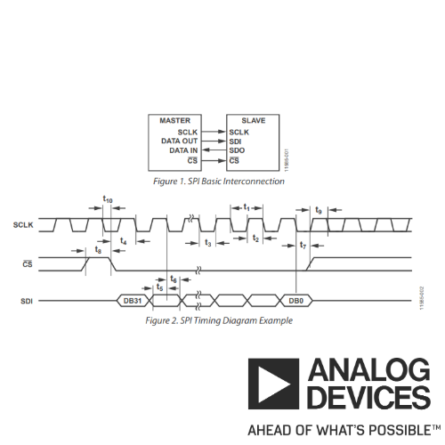
AN-1248: SPI Interface
Analog Devices Inc.The SPI bus interface is extensively employed for synchronous data transmission due to its ability to support relatively high transmission rates with versatile configurations.
While the SPI has attained de facto standard status, it lacks de jure standardization, meaning it is not officially specified. While this lack of formal specification can be advantageous, allowing designers to optimize functionality, it does introduce complexities in interconnecting different parts.
The SPI bus comprises four unidirectional wires, with varying names for these wires across different parts, even within the same product range.
- Interface enable: CS, SYNC, ENABLE, etc.
- Data in: SDI, MISO (for master), MOSI (for slave), etc.
- Data out: SDO, MISO (for slave), MOSI (for master), etc.
- Clock: SCLK, CLK, SCK, etc.


