AN-1354 - Integrated ZIF, RF to Bits, LTE, Wide Area Receiver Analysis and Test Result
Analog Devices Inc.This application note references the 3GPP TS 36 series documents and various Analog Devices, Inc., data sheets, characterization reports, and lab test results. The key focus is on the analysis and test result of an integrated, zero intermediate frequency (ZIF), RF to bits, IC (AD9371) based radio receiver for multicarrier, wide area LTE operations.
AN-105 - Current Sense Circuit Collection Making Sense of Current
Analog Devices Inc.Sensing and/or controlling current flow is a fundamental requirement in many electronics systems, and the techniques to do so are as diverse as the applications themselves. This Application Note compiles solutions to current sensing problems and organizes the solutions by general application type. These circuits have been culled from a variety of Linear Technology documents.
.png)
AN-2554: Step Counting Using the ADXL367
Analog Devices Inc.This application note describes the implementation of a pedometer algorithm for the ADXL367, a 3-axis digital accelerometer. The algorithm is based on peak detection analysis of the acceleration produced by a step over a predefined time window. Empirical results for a wrist worn use case show approximately 97% average accuracy under different scenarios.
AN-617: Wafer Level Chip Scale Package (WLCSP)
Analog Devices Inc.The Wafer Level Chip Scale Package (WLCSP) represents a cutting-edge variant of the flip-chip interconnection technique, wherein all packaging processes are completed at the wafer level. WLCSPs employ solder balls to connect the inverted active side of the die to the printed circuit board (PCB). Notably, the size of these solder balls, typically ranging from 250 μm to 300 µm pre-reflow, renders underfill unnecessary in comparison to conventional flip-chip interconnects.
This innovative interconnection technology offers several key advantages, enhancing both performance and efficiency:
- Significant space savings are achieved by eliminating the first-level package components (mold compound, lead frame, or organic substrate). For instance, an 8-bump WLCSP occupies merely 8% of the board area consumed by an 8-lead SOIC.
- Improved electrical performance, including reduced inductance, stems from eliminating wire bonds and leads inherent in standard plastic packaging.
- The package boasts a lighter weight and thinner profile due to the absence of a lead frame and molding compound.
- High assembly yields are ensured by the self-aligning characteristic of the low-mass die during solder attachment.
The primary purpose of this application note is to furnish end-users with comprehensive information covering WLCSP construction, configurations, dimensions, PCB design, surface-mount guidelines, reliability, thermal performance, rework procedures, and shipping media. This resource is designed to provide valuable insights into maximizing the benefits of WLCSP technology for optimized electronic packaging solutions.
AN-1314: AMR Angle Sensors
Analog Devices Inc.Anisotropic Magnetoresistive (AMR) thin film materials are gaining increasing significance in contemporary position sensing technologies. Magnetoresistive (MR) position measurement offers numerous advantages compared to traditional methods, with reliability, accuracy, and overall robustness being key factors driving the advancement of MR sensing technologies. Features such as low cost, compact size, contactless operation, wide temperature range, dust and light insensitivity, and operation across a broad magnetic field spectrum collectively contribute to a resilient sensor design.
The MR effect, which involves a material altering its electrical resistance in response to changes in the direction or magnitude of an externally applied magnetic field, forms the foundation of AMR materials. These materials operate in two distinct areas: high field and low field. This application note focuses on high field applications, where the externally applied magnetic field far exceeds the internal field of the sensor, leading to saturation. In saturation mode, the change in resistance is solely dependent on the field direction, irrespective of the applied field strength.
Owing to the characteristics of AMR films, the resistance change for opposing directions is identical, making it challenging for the sensor to differentiate between a north and south magnetic pole. Consequently, the output information for a single rotating dipole magnet repeats twice over a complete mechanical revolution, limiting the measurement range to 180°. The change in resistance is mathematically modeled by the equation:

where:
R is the sensor resistance.
R0 is the unexcited sensor resistance.
ΔR0 is the change in sensor resistance.
For AMR sensors, in general, ΔR0 is approximately 3% of the overall resistance of the bridge. Due to this modest change in resistance, an instrumentation amplifier becomes essential to further amplify the output signal to a usable value proportional to the supply voltage.
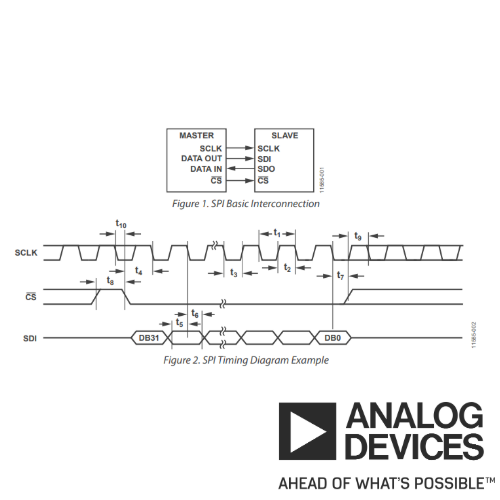
AN-1248: SPI Interface
Analog Devices Inc.The SPI bus interface is extensively employed for synchronous data transmission due to its ability to support relatively high transmission rates with versatile configurations.
While the SPI has attained de facto standard status, it lacks de jure standardization, meaning it is not officially specified. While this lack of formal specification can be advantageous, allowing designers to optimize functionality, it does introduce complexities in interconnecting different parts.
The SPI bus comprises four unidirectional wires, with varying names for these wires across different parts, even within the same product range.
- Interface enable: CS, SYNC, ENABLE, etc.
- Data in: SDI, MISO (for master), MOSI (for slave), etc.
- Data out: SDO, MISO (for slave), MOSI (for master), etc.
- Clock: SCLK, CLK, SCK, etc.
AN-931 - Understanding PulSAR ADC Support Circuitry
Analog Devices Inc.Successive approximation register (SAR) analog-to-digital converters (ADCs) use various new techniques for improved resolution. Understanding how these devices work is important in preventing malfunction and erroneous issues. This application note discusses in general the pitfalls that occur regularly when using SAR ADCs and, more importantly, how to easily prevent them.
AN-202 - An IC Amplifier User’s Guide to Decoupling, Grounding, and Making Things Go Right for a Change
Analog Devices Inc.An IC Amplifier User’s Guide to Decoupling, Grounding, and Making Things Go Right for a Change

AN6488 - Achieving Desired Dynamic Performance in High-Speed, High-Resolution ADCs with Level Translators/Isolators in the System
Analog Devices Inc.Communicating with ADCs above 500ksps is tough. Adding another variable such as a level translator or isolator to the SPI communication requires more understanding of timing and modifying hardware and firmware. This application note discusses how to achieve the desired dynamic performance with level translators or isolators.
AN-7657 - Using the MAX66250 Desktop Application, the Basics
Analog Devices Inc.This application note walks through the basics of the MAX66250 NFC/RFID device in terms of its use with the associated desktop application. The functionality of the IC is exercised using the development mode of the software, which allows for the configuration of programs to enable the communication, memory, and protection features of the device. Furthermore, the results of these programs can be logged and interpreted in the operator mode of the software.
AN7650 - How to Optimize the Frequency Response of Buck Regulator ICS Externally
Analog Devices Inc.This application note describes how external compensation works and provides a method to implement it with above-mentioned devices. Through external compensation, the frequency response of buck switching regulators is adjusted to increase or decrease the bandwidth of the system by addition of a simple RC network with a feedback circuit.
AN-940 - Low Noise Amplifier Selection Guide for Optimal Noise Performance
Analog Devices Inc.When evaluating an amplifier’s performance for a low noise application, both internal and external noise sources must be considered. This application note briefly discusses the fundamentals of both internal and external noise and identifies the tradeoffs associated in selecting the optimal amplifier for low noise design.


