Description
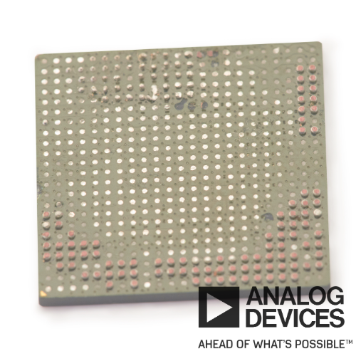
The Wafer Level Chip Scale Package (WLCSP) represents a cutting-edge variant of the flip-chip interconnection technique, wherein all packaging processes are completed at the wafer level. WLCSPs employ solder balls to connect the inverted active side of the die to the printed circuit board (PCB). Notably, the size of these solder balls, typically ranging from 250 μm to 300 µm pre-reflow, renders underfill unnecessary in comparison to conventional flip-chip interconnects.
This innovative interconnection technology offers several key advantages, enhancing both performance and efficiency:
- Significant space savings are achieved by eliminating the first-level package components (mold compound, lead frame, or organic substrate). For instance, an 8-bump WLCSP occupies merely 8% of the board area consumed by an 8-lead SOIC.
- Improved electrical performance, including reduced inductance, stems from eliminating wire bonds and leads inherent in standard plastic packaging.
- The package boasts a lighter weight and thinner profile due to the absence of a lead frame and molding compound.
- High assembly yields are ensured by the self-aligning characteristic of the low-mass die during solder attachment.
The primary purpose of this application note is to furnish end-users with comprehensive information covering WLCSP construction, configurations, dimensions, PCB design, surface-mount guidelines, reliability, thermal performance, rework procedures, and shipping media. This resource is designed to provide valuable insights into maximizing the benefits of WLCSP technology for optimized electronic packaging solutions.