AN4889 - Using Core Independent Peripherals (CIPs) to Implement a Peltier Cooled Metal Plate
Microchip Technology Inc.Core Independent Peripherals (CIPs) are specially designed hardware blocks inside a microcontroller (MCU) that add new capabilities, reduce code and improve system performance. This application note will showcase an example of this by discussing the design elements, decisions and logic that went into building a Peltier Cooled Metal Plate with only one microcontroller: a 20-pin PIC16F17146.
AN4495 - MPLAB Harmony v3 Project Migration
Microchip Technology Inc.This document discusses the migration of an existing MPLAB Harmony v3 based project developed on a particular hardware (microcontroller or development board) platform to another one of Microchip's 32-bit hardware platforms of the user's choice.
AN4591 - PolarFire FPGA Implementing Data Security Using User Cryptoprocessor Application Note
Microchip Technology Inc.PolarFire FPGAs represent the industry's most advanced security programmable FPGAs. Data security protects application data—stored, communicated, or computed at run-time—from being copied, altered, or corrupted.
AN4576 - PolarFire DisplayPort Tx Solution with Camera Video Output Application Note
Microchip Technology Inc.This document describes how to run the imaging and video demo using the PolarFire video kit, with a single camera sensor from the dual-sensor module and a DisplayPort Tx. The demo design features a fully integrated solution developed using Microchip’s Libero® System-on-Chip (SoC) software to help customers evaluate PolarFire FPGA in smart embedded vision applications and to build prototypes quickly.
AN4827 ATmegaS128 IO Expander
Microchip Technology Inc.This application note describes the implementation of a Radiation Tolerant Port Expander application using the Serial Peripheral Interface (SPI) interface on the ATmegaS family of space-qualified AVR Microcontrollers (MCUs). The goal is to functionally emulate the MCP23S17. The ATmegaS128 is a function and pin-identical variant of the ATmega128 commercial device, and it ensures a full code and toolchain compatibility.
AN4383 - 32-bit Microcontroller Wafer-Level Chip-Scale Package (WLCSP)
Microchip Technology Inc.This document provides Microchip's 32 MCU Wafer-Level Chip-Scale Packages (WLCSP) information. It gives details such as bootloader, programming, and ordering guidelines. It also includes information on handling, shipping, SMT, and rework.
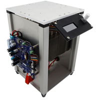
AN4888 - Innovative Mounting Techniques Enhance Thermal Performance of the Surface-Mount D3PAK Package
Microchip Technology Inc.The D3PAK surface-mount power package accommodates silicon chips with dimensions up to 416 × 270 mils. Such chips, when housed in the TO-247 package, can dissipate up to 360W at a case temperature of 25°C. However, these same chips are limited to less than 7W at 25°C ambient, when housed in a D3PAK and soldered to a standard FR-4 printed circuit board (PCB). Clearly, any technique capable of boosting the D3PAK dissipation capability nearer to the TO-247 benchmark merits close attention.
This application note will compare the thermal performance of various mounting methods for the D3PAK including classic surface mount device (SMD) printed circuit board mounting; insulated metal substrate (IMS) mount down, with and without an attached heat sink; oven-fired ceramic substrate, with and without heat sink; and direct bonded copper (DBC) substrates, with and without heat sink.
The importance of optimized bonding will be explored, independent of the actual substrate used, covering choice of appropriate solder alloys and fluxes, as well as the layout of the interface metallization patterns to preclude voiding during reflow operations.
Finally, a relative cost versus performance evaluation will be presented on the various methods described in the paper.
AN3782 - RT PolarFire: TMR and Spatial Separation for Higher Reliability
Microchip Technology Inc.The purpose of this application note is to help FPGA designers to implement the Triple Module Redundancy (TMR) design technique on a VHDL design, which is targeted on a Microchip Radiation-Tolerant PolarFire (RT PolarFire) FPGA.
This application note describes how to implement each logical register with a TMR register on different hierarchies of a VHDL/Verilog design. It shows how to use the syn_radhardlevel synthesis attribute on the architecture and signal on different hierarchies.
These design example projects are targeted towards use in a RTPF500T-CG1509M device (Rad-Tolerant PolarFire FPGA, 500K Logic-Elements with High-Speed Serial Transceivers in a Ceramic Column Grid Array Package with 1509 solder columns).
AN4903 - Differences Between RT PolarFire RTPF500T and RTPF500ZT FPGAs
Microchip Technology Inc.Radiation-Tolerant (RT) PolarFire FPGAs are derived from PolarFire 28 nm non-volatile and reprogrammable FPGA devices from Microchip.
This document summarizes the differences between the RTPF500T and RTPF500ZT device versions.
AN3589 - Using Sigma-Delta Analog-to-Digital Converter on SAMC MCU with MPLAB Harmony v3
Microchip Technology Inc.This application note describes the Sigma-Delta Analog-to-Digital Converter (SDADC) in ATSAMC21N device is configured in differential mode and the SDADC results are displayed on a console. It also provides example code for both interrupt and polling methods, developed using MPLAB® X IDE and MPLAB Harmony v3 Configurator
AN3475 - File Transfer Protocol Using MPLAB Harmony v3 TCP/IP Stack
Microchip Technology Inc.This document focuses on the FTP implementation of the MPLAB® Harmony v3 TCP/IP stack, available in the latest MPLAB Harmony v3 framework. It also provides an FTP client demonstration using the SAM E70 microcontroller. This demonstration implements an Ethernet bootloader using FTP, through which the SAM E70 client downloads a binary for self-programming from an FTP server.
AN3466 - Using XDMAC with QSPI on Arm Cortex-M7 MCUs Using MPLAB Harmony v3
Microchip Technology Inc.This document describes how to use the Direct Memory Access Controller (XDMAC) with the Quad Serial Peripheral Interface (QSPI) on a Arm®Cortex®-M7 based MCU (SAM E70). It also describes the implementation of an application using the MPLAB® Harmony v3 Software Framework, and evaluates performance of QSPI read and write operations with or without XDMAC.
AN3508 - Dual Bank Bootloader on SAM E54 Microcontroller (MCU) Using MPLAB Harmony v3
Microchip Technology Inc.The bootloader is a piece of code used to program or re-program the application code (firmware) to the internal Flash of the microcontroller without the need for an external programmer or debugger.
This document describes the dual-bank bootloader provided by MPLAB Harmony v3. The dual-bank bootloader utilizes the dual-bank feature of the internal Flash for safer application upgrade.
AN1294 - PTP Calibration Configuration Guide
Microchip Technology Inc.This configuration guide provides information on how to make Port-to-port and 1PPS calibrations to improve timing by adjusting the ingress/egress latencies.
AN4792 - PolarFire FPGA: High-Speed Data Transfer in 8b10B Mode Using the LiteFast IP (Earlier DG0783)
Microchip Technology Inc.This document describes how to run the LiteFast IP demo on the PolarFire® Evaluation Board using the LiteFast GUI application.
AN4833 - File Transfer Protocol Using MPLAB Harmony v3 TCP/IP Stack for SAM E54 MCU
Microchip Technology Inc.The File Transfer Protocol (FTP) is a standard internet protocol provided by TCP/IP for transmitting files from one device to another. It is an application layer protocol within the TCP/IP stack layers. An embedded FTP client/server is an excellent addition to any network-enabled device. The FTP client module will enable your application to upload and download files from any FTP server. This protocol enables data transfer reliably and efficiently between different devices without worrying about the file storage systems of a Host.
This document focuses on the FTP implementation of the MPLAB Harmony v3 TCP/IP stack. It also provides a combined FTP client and FTP server demonstration using the SAM E54 microcontroller. The FTP client application has an Ethernet bootloader that downloads the application binary from the FTP server and updates the firmware by self-programming.
AN4947: Building Mi-V Processor Subsystem for RTG4 FPGA Application Note (Earlier AC490)
Microchip Technology Inc.This application note describes how to build a Mi-V processor subsystem to execute a user application from the designated fabric RAMs or DDR memory.
AN4892: RTG4 SRAM Initialization After Powerup Using μPROM Application Note (AC454)
Microchip Technology Inc.This application note describes how to initialise the Static Random Access Memory (SRAM) blocks of Microchip RTG4 Field Programmable Gate Array (FPGA) with user data after power-up. The design for this application note uses a Large SRAM (LSRAM) block, which is initialised by an FPGA fabric master through the Advanced Microcontroller Bus Architecture Advanced Peripheral Bus interface (AMBA APB bus).
RTG4 FPGA devices have embedded SRAM blocks (LSRAM and µSRAM) in the fabric. Both LSRAM and µSRAM blocks are placed in multiple rows within the FPGA fabric, and they can be accessed through the fabric routing architecture.
AN4686 - Watchdog Timer (WDT) on ATSAM E70/S70/V70/V71 Devices Using MPLAB Harmony v3
Microchip Technology Inc.This document discusses the WDT theory of operations, modes, and clock sources. It also covers configuration and code generation using MPLAB Harmony v3.
AN4900 - bPHY-EXERCISER
Microchip Technology Inc.Microchip’s bPHY Exerciser is a test platform that is used for conformance testing, specifically when conducting a limited physical layer verification. The test platform supports the execution of balanced media physical layer (bPHY) conformance tests in 50 Mbit/s INICnet technology networks. The bPHY Exerciser mainly consists of the bPHY Exerciser hardware and a software that can be used to configure various test scenarios. This document explains you how to setup the test environment, establish required connections and perform specific measurements.


