GPS Tracking Using Sub-1GHz Devices
Texas Instruments
Waveform Capture Based Approach for Ultrasonic Sensing Technology for Flow Meter
Texas InstrumentsThis FAQ describes the ADC-based correlation techniques for time-of-flight measurements used in ultrasonic-sensing technology for flow metering. This document describes the design and engineering trade-offs when designing using the MSP430FR604x microcontrollers (MCUs), software based on the Ultrasonic Design Center, and key performance metrics.

Sensorless-FOC With Flux-Weakening and MTPA for IPMSM Motor Drives
Texas Instruments
Robust Isolated RS-485 enables new industrial applications
Texas InstrumentsRS-485 is one of the most widely used wired interface for industrial long-haul networks. TIA/EIA-485-A standard defines the physical layer of the RS-485 interface. End applications use RS-485 interface coupled with protocol such as Profibus, Modbus or BACnet.
The main benefits of this interface include:
- Balanced differential signaling allows for rejection of common mode noise and facilitates communications over long distances in noisy industrial environments.
- Support of -7 to 12V wide common mode range allows for multipoint data transmission between nodes located at different ground potential difference.
- Data rates up to 50 Mbps at short distances or communications distance up to 1000 meters at slower data rates is possible.
Applications for RS-485 include Energy Meters, Grid Protection relay, Solar inverter, Factory automation, Motor control and Heating, ventilation, air conditioning (HVAC) systems.

Two-channel, K-type thermocouple measurement circuit with internal temperature
Texas InstrumentsThis cookbook design describes a temperature measurement circuit with two thermocouples using the ADS1118. Thermocouple voltage measurements are made with the ADS1118 internal voltage reference, while cold-junction compensation (CJC) measurements are made with the onboard temperature sensor. Two channels of the ADC are used for two K-type thermocouples with a temperature measurement range from –270°C to 1370°C. Included in this design are ADC register settings to configure the device and pseudo code is provided to configure and read from the device. This circuit can be used in applications such as analog input modules for PLCs, lab instrumentation, and factory automation.
.jpg)
Inverting Application for the LMZM33604/6
Texas InstrumentsThe LMZM33606 is a 16 × 10 mm2 6-A rated synchronous step-down power module that features a wide operating input range from 3.5 V to 36 V with adjustable output voltage range from 1 V to 20 V. The LMZM33606 can be configured in an inverting buck-boost (IBB) topology with the output voltage inverted or negative with respect to input voltage. This application report shows how the conventional non-inverting evaluation board for the LMZM33606 can be configured for an inverting application. This application note also provides the additional level-shifter circuitry for EN and PGOOD pin if the feature is required. Note that the LMZM33604 is rated for 4A and pin-to-pin compatible with the LMZM33606.
Tamper Detector
Dialog SemiconductorTamper detection is a function widely used within critical infrastructure systems such as power meters, water meters, security and fire panels, and any other products where a trigger input needs to be detected and the event recorded in non-volatile memory (Flash memory). The SLG46811 GreenPAK mixed-signal IC is ideally suited for this tamper-detection role when paired with the AT45DB161E Flash memory for recording the event.
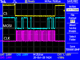
AN3703 - Live Update Application on PIC32MZ MCUs Using MPLAB Harmony v3
Microchip Technology Inc.The dual-panel Flash on the PIC32MZ microcontroller (MCU) allows the application to implement the Live Update features. The Live Update feature is a piece of code used to program the application code (firmware) to the inactive bank in the internal Flash or non-volatile memory (NVM).
AN1180 - DGD05463 DGD0506A Application Note
Diodes Inc.The DIODES DGD05463 and DGD0506A high-frequency, half-bridge gate drivers with programmable deadtime are used to optimally drive the gate of MOSFETs. The DGD05463/06A respectively have an integrated bootstrap diode for ease of design and lower BOM.
Configuring The Raspberry Pi Compute Module 4
Raspberry PiThis document describes how to disable various hardware interfaces, in both hardware and software, and how to reduce the amount of memory used by the Linux operating system (OS).
Fleet Management - A Brief Introduction
Raspberry PiAs Raspberry Pi devices become more commonplace as part of a company’s portfolio of devices, there becomes a need to manage these devices.
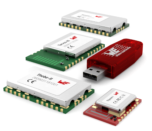
ANR022 - Radio module cross migration guide
Wurth ElektronikThis application note describes an adapter board, that is used to place a 2.4 GHz Thyone-I radio module on the footprint of a Tarvos-III/Telesto-III/Thebe-II/Themisto-I radio module.
Furthermore, the steps for hardware and firmware integration to replace an existing Tarvos-III/Telesto-III/Thebe-II/Themisto-I radio module by a Thyone-I radio module are described.
ANP008 - Negative input resistance of switching regulators
Wurth ElektronikDevelopers of switching regulators and switch mode power supplies attach great importance to the efficiency of their circuits. However, at the end of their development phase, they encounter unpleasant effects such as unwanted oscillations at the input of the switching regulator and these although the switching regulator produces a constant output voltage under all conditions. But why does the input of the switching regulator tend to oscillation under certain circumstances?

AKX01100-1 - Thermal Design for Schottky Barrier Diodes (SBDs) in the US2H Package
Toshiba Electronics EuropeThermal Design for Schottky Barrier Diodes (SBDs) in the US2H Package
The US2H package is a thermally enhanced package specifically designed for diodes. This application note describes the advantages of Schottky barrier diodes (SBDs) in the US2H package as well as the power losses of and the thermal design for SBDs.
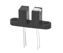
App-Note-201 - Motion Sensing With Interrupters
TT electronics plcThis application bulletin will discuss many of the variables associated with single channel encoding. This will include design considerations for using booth non-aperture and aperture transistors or Photologic® output devices. Refer to application bulletins 203 and 206 for additional information.
App-Note-204 - Reflective Assemblies Design Considerations
TT electronics plcA reflective assembly generally consists of a single emitter and sensor in the same housing. This provides a major mounting advantage because optical access to the surface to be sensed is required from only one side. However, this can lead to a wide variety of design variables involving mounting configurations, reflective surface, and sensing circuits.
AN1175 - DGD2110 DGD2113 Application Note
Diodes Inc.The DIODESTM DGD2110/2113 are High Side/Low Side gate drivers used to optimally drive the gate of MOSFETs or IGBTs. For the DGD2110, the high-side floating well has a maximum operation of 500V; and for the DGD2113, the high-side floating well has a maximum operation of 600V.
AN1174 - DGD0579U Application Note
Diodes Inc.The DIODES DGD0579U, High-side/Low-side gate driver with Integrated Bootstrap Diode is used to optimally drive the gate of MOSFETs. Below is an example application using DGD0579U with MOSFETs to make three Half-bridge circuits used to drive a BLDC motor. The DGD0579U is also well-suited to low voltage power supplies due to its high-speed performance. In this document, the important parameters needed to design in the DGD0579U are discussed. Main sections are bootstrap capacitor selection, gate driver component selection, decoupling capacitor discussion, and PCB layout suggestions.
AN1170 - DGD0215 DGD0216 and DGD0211C Application Note
Diodes Inc.The DGD0215/16 and DGD0211C are High-Speed, Low-Side Gate Drivers, capable of source current of 1.9A and sink current of 1.8A. Low-Side Gate Drivers will optimally charge the gate of MOSFETs or IGBTs in a ground-based configuration.
AN1168 - DGD2101M Application Note
Diodes Inc.The DGD2101M, High-side/Low-side gate driver is used to optimally drive the gate of MOSFETs or IGBTs. Below (Figure 1) is an example application using DGD2101M with MOSFETs to make three Half-bridge circuits used to drive a three phase motor. Typical motor applications are AC Induction motors, PMSMs, and BLDC motors. DGD2101M can also be used in power supplies. In this document, the important parameters needed to design in the DGD2101M are discussed. Main sections are bootstrap resistor, diode, and capacitor selection, gate driver component selection, decoupling capacitor discussion, and PCB layout suggestions.


