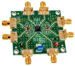
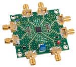
Top Manufacturers
Stock

Displaying 1101 - 1120 of 5453

Evaluation Kits from Analog Devices Inc.

AD9253-125EBZ

Analog Devices Inc.
The AD9253 is a quad, 14-bit, 80 MSPS/105 MSPS/125 MSPSanalog-to-digital converter (ADC) with an on-chip sample-and-holdcircuit designed for low cost, low power, small size,and ease of use. The product operates at a conversion rate ofup to 125 MSPS and is optimized for outstanding dynamicperformance and low power in applications where a smallpackage size is critical.The ADC requires a single 1.8 V power supply and LVPECL-/CMOS-/LVDS-compatible sample rate clock for full performanceoperation. No external reference or driver components arerequired for many applications.The ADC automatically multiplies the sample rate clock for theappropriate LVDS serial data rate. A data clock output (DCO) forcapturing data on the output and a frame clock output (FCO)for signaling a new output byte are provided. Individual-channelpower-down is supported and typically consumes less than 2 mWwhen all channels are disabled. The ADC contains several featuresdesigned to maximize flexibility and minimize system cost, such as programmable output clock and data alignment and digitaltest pattern generation. The available digital test patternsinclude built-in deterministic and pseudorandom patterns, alongwith custom user-defined test patterns entered via the serial portinterface (SPI).The AD9253 is available in a RoHS-compliant, 48-lead LFCSP.It is specified over the industrial temperature range of ?40?C to+85?C. This product is protected by a U.S. patent.PRODUCT HIGHLIGHTS Small Footprint. Four ADCs are contained in a small, spacesaving package. Low power of 110 mW/channel at 125 MSPS with scalable power options. Pin compatible to the AD9633 12-bit quad ADC. Ease of Use. A data clock output (DCO) operates at frequencies of up to 500 MHz and supports double data rate (DDR) operation. User Flexibility. The SPI control offers a wide range of flexible features to meet specific system requirementsAPPLICATIONS Medical imaging and nondestructive ultrasound Quadrature radio receivers Diversity radio receivers Optical networking Test equipment

DC1293A

Analog Devices Inc.
The LT1939 is a current mode PWM step-down DC/DC converter with an internal 2.3A switch. The wide input range of 3V to 25V makes the LT1939 suitable for regulating power from a wide variety of sources, including automotive batteries, industrial supplies and unregulated wall adapters.Resistor-programmable 250kHz to 2.2MHz frequency range and synchronization capability enable optimization between efficiency and external component size. Cycle-by-cycle current limit, frequency foldback and thermal shutdown provide protection against a shorted output. The soft-start feature controls the ramp rate of the output voltage, eliminating input current surge during start-up, and also provides output tracking.The LT1939 contains an internal NPN transistor with feedback control which can be con?gured as a linear regulator or as a linear regulator controller.The LT1939?s low current shutdown mode (

ADP1853-EVALZ

Analog Devices Inc.
The ADP1853 is a wide range input, dc-to-dc, synchronousbuck controller capable of running from commonly used 3.3 Vto 12 V (up to 20 V) voltage inputs. The device nominallyoperates in current mode with valley current sensing providingthe fastest step response for digital loads. It can also beconfigured as a voltage mode controller with low noise andcrosstalk for sensitive loads.The ADP1853 can be used as a master synchronization clockfor the power system and for convenient synchronizationbetween controllers. The CLKOUT signal can synchronizeother devices in the ADP185x family such that slave devicesare phase-shifted from the master to reduce the input ripplecurrent, improve EMI, and reduce the size of the input bulkcapacitance. The ADP1853 can also be configured as a slavedevice for current sharing. Additionally, the ADP1853 includesaccurate tracking, precision enable, and power good functionsfor sequencing. The ADP1853 provides a high speed, high peakcurrent gate driving capability to enable energy efficient powerconversion. The device can be configured to operate in powersaving mode by skipping pulses, reducing switching losses andimproving efficiency at light load and standby conditions.The accurate current limit allows design within a narrowerrange of tolerances and can reduce overall converter size andcost. The ADP1853 can regulate down to 0.6 V output using ahigh accuracy reference with ?1% tolerance over thetemperature range from ?40?C to 125?C.With a wide range input voltage, the ADP1853 is designed toprovide the designer with maximum flexibility for use in avariety of system configurations; loop compensation, soft start,frequency setting, power saving mode, current limit, andcurrent sense gain can all be programmed using externalcomponents. In addition, the external RAMP resistor allowschoosing optimal slope and VIN feedforward in both currentand voltage mode for excellent line rejection. The linearregulator and the boot strap diode for the high-side driver areinternal.Protection features include undervoltage lock out, overvoltage,overcurrent/short circuit, and overtemperature.Applications Intermediate bus and POL systems requiring sequencing and tracking, including Telecom base station and networking Industrial and Instrumentation Medical and healthcare

EVAL-AD7170EBZ

Analog Devices Inc.
The AD7170 is a very low power 12-bit analog-to-digital converter (ADC). It contains a precision 12-bit sigma-delta (?-?) ADC and an on-chip oscillator. Consuming only 135 ?A, the AD7170 is particularly suitable for portable or battery operated products where very low power is a requirement. The AD7170 also has a power-down mode in which the device consumes 5 ?A, thus increasing the battery life of the product.For ease-of-use, all the features of the AD7170 are controlled by dedicated pins. Each time a data read occurs, eight status bits are appended to the 12-bit conversion. These status bits contain a pattern sequence that can be used to confirm the validity of the serial transfer.The output data rate of the AD7170 is 125 Hz, whereas the settling time is 24 ms. The AD7170 has one differential input and a gain of 1. This is useful in applications where the user needs to use an external amplifier to implement system-specific filtering or gain requirements.The AD7170 operates with a power supply from 2.7 V to 5.25 V. It is available in a 10-lead LFCSP package.The AD7171 is a 16-bit version of the AD7170. It has the same feature set as the AD7170 and is pin-for-pin compatible.INTERFACE 2-wire serial (read-only device) SPI compatible Schmitt trigger on SCLKAPPLICATIONS Pressure measurement Industrial process control Portable instrumentation

EVAL-AD5172SDZ

Analog Devices Inc.
The AD5172 / AD5173?are dual-channel, 256-position, one-time programmable (OTP) digital potentiometers that employ fuse link technology to achieve memory retention of resistance settings. The digital potentiometer, VR, and RDAC terms are used interchangeably. OTP is a cost-effective alternative to EEMEM for users who do not need to program the digital potentiometer setting in memory more than once. These devices perform the same electronic adjustment function as mechanical potentiometers or variable resistors but with enhanced resolution, solid-state reliability, and superior low temperature coefficient performance.TheAD5172 / AD5173 are programmed using a 2-wire, I2C-compatible digital interface. Unlimited adjustments are allowed before permanently setting the resistance value. During OTP activation, a permanent blow fuse command freezes the wiper position (analogous to placing epoxy on a mechanical trimmer).Unlike traditional OTP digital potentiometers, the AD5172 / AD5173 have a unique temporary OTP overwrite feature that allows for new adjustments even after a fuse is blown. However, the OTP setting is restored during subsequent power-up conditions. This allows users to treat these digital potentiometers as volatile potentiometers with a programmable preset.APPLICATIONS Systems calibration Electronics level setting Mechanical trimmers replacement in new designs Permanent factory PCB setting Transducer adjustment of pressure, temperature, position, chemical, and optical sensors RF amplifier biasing Gain control and offset adjustment
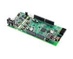
ADP5023CP-EVALZ

Analog Devices Inc.
The ADP5023 combines two high performance buck regulators and one low dropout (LDO) regulator in a small, 24-lead 4 mm ? 4 mm LFCSP to meet demanding performance and board space requirements.The high switching frequency of the buck regulators enables tiny multilayer external components and minimizes the board space. When the MODE pin is set high, the buck regulators operate in forced PWM mode. When the MODE pin is set low, the buck regulators operate in PWM mode when the load current is?above a predefined threshold. When the load current falls below a predefined threshold, the regulator operates in power save mode (PSM) improving the light-load efficiency.The two bucks operate out of phase to reduce the input capacitor requirement. The low quiescent current, low dropout voltage, and wide input voltage range of the ADP5023 LDO extends the battery life of portable devices. The ADP5023 LDO maintains power supply rejection greater than 60 dB for frequencies as high as 10 kHz while operating with a low headroom voltage.Regulators in the ADP5023 are activated though dedicated enable pins. The default output voltages can be externally set in the adjustable version or factory programmable to a wide range of preset values in the fixed voltage version.Applications Power for processors, ASIC, FPGAs, and RF chipsets Portable instrumentation and medical devices Space constrained devices

LTC3810EG Demo Board | 13V ≤ VIN ≤ 80V; VOUT = 12V @ 6A

Analog Devices Inc.
Demonstration circuit 952 is a current mode synchronous switching regulator featuring the LTC3810. The circuit is configured as a synchronous step-down regulator operating at 230kHz switching frequency. Output voltage is 12V at 6A maximum load. The input voltage range is 13V to 80V.

DC2296A-KIT

Analog Devices Inc.
The LTC2983 measures a wide variety of temperature sensors and digitally outputs the result, in ?C or ?F, with 0.1?C accuracy and 0.001?C resolution. The LTC2983 can measure the temperature of virtually all standard (type B, E, J, K, N, S, R, T) or custom thermocouples, automatically compensate for cold junction temperatures and linearize the results. The device can also measure temperature with standard 2-, 3- or 4-wire RTDs, thermistors and diodes. It has 20 reconfigurable analog inputs enabling many sensor connections and configuration options. The LTC2983 includes excitation current sources and fault detection circuitry appropriate for each type of temperature sensor.The LTC2983 allows direct interfacing to ground referenced sensors without the need for level shifters, negative supply voltages, or external amplifiers. All signals are buffered and simultaneously digitized with three high accuracy, 24-bit ?? ADCs, driven by an internal 10ppm/?C (maximum) reference.Applications Direct Thermocouple Measurements Direct RTD Measurements Direct Thermistor Measurements Custom Sensor Applications

AD8039ART-EBZ

Analog Devices Inc.
The AD8038 (single) and AD8039 (dual) amplifiers are high speed (350 MHz) voltage feedback amplifiers with an exceptionally low quiescent current of 1.0 mA/amplifier typical (1.5 mA maximum). The AD8038 single amplifier in the 8-lead SOIC package has a disable feature. Despite being low power and low cost, the amplifier provides excellent overall performance. Additionally, it offers a high slew rate of 425 V/?s and a low input offset voltage of 3 mV maximum.The Analog Devices, Inc., proprietary XFCB process allows low noise operation (8 nV/?Hz and 600 fA/?Hz) at extremely low quiescent currents. Given a wide supply voltage range (3 V to 12 V), wide bandwidth, and small packaging, the AD8038 and AD8039 amplifiers are designed to work in a variety of applications where power and space are at a premium.The AD8038 and AD8039 amplifiers have a wide input common-mode range of 1 V from either rail and swing to within 1 V of each rail on the output. These amplifiers are optimized for driving capacitive loads up to 15 pF. If driving larger capacitive loads, a small series resistor is needed to avoid excessive peaking or overshoot.The AD8039 amplifier is available in a 8-lead SOT-23 package, and the single AD8038 is available in both an 8-lead SOIC and a 5-lead SC70 package. These amplifiers are rated to work over the industrial temperature range of ?40?C to +85?C.Applications Battery-powered instrumentation Filters A/D drivers Level shifting Buffering Photo multipliers

EVAL-AD5371EBZ

Analog Devices Inc.
The AD5371 contains 40 14-bit DACs in a single 80-lead LQFP or 100-ball CSP_BGA. The device provides buffered voltage outputs with a span of 4? the reference voltage. The gain and offset of each DAC can be independently trimmed to remove errors. For even greater flexibility, the device is divided into five groups of eight DACs. Three offset DACs allow the output range of the groups to be adjusted. Group 0 can be adjusted by Offset DAC 0, Group 1 can be adjusted by Offset DAC 1, and Group 2 to Group 4 can be adjusted by Offset DAC 2.The AD5371 offers guaranteed operation over a wide supply range, with VSS from ?16.5 V to ?4.5 V and VDD from 9 V to 16.5 V. The output amplifier headroom requirement is 1.4 V operating with a load current of 1 mA.The AD5371 has a high speed serial interface that is compatible with SPI, QSPI?, MICROWIRE?, and DSP interface standards and can handle clock speeds of up to 50 MHz. It also has a 100 MHz low voltage differential signaling (LVDS) serial interface.The DAC registers are updated on reception of new data. All the outputs can be updated simultaneously by taking the LDAC input low. Each channel has a programmable gain and an offset adjust register to allow removal of gain and offset errors.Each DAC output is gained and buffered on chip with respect to an external SIGGNDx input. The DAC outputs can also be switched to SIGGNDx via the CLR pin.APPLICATIONS Level setting in automatic test equipment (ATE) Variable optical attenuators (VOA) Optical switches Industrial control systems Instrumentation

AD8304-EVALZ

Analog Devices Inc.
The AD8304 is a monolithic logarithmic detector optimized for the measurement of low frequency signal power in fiber optic systems. It uses an advanced translinear technique to provide an exceptionally large dynamic range in a versatile and easily used form. Its wide measurement range and accuracy are achieved using proprietary design techniques and precise laser trimming. In most applications only a single positive supply, VP, of 5 V will be required, but 3.0 V to 5.5 V can be used, and certain applications benefit from the added use of a negative supply, VN. When using low supply voltages, the log slope is readily altered to fit the available span. The low quiescent current and chip disable features facilitate use in battery-operated applications.The AD8304 is available in a 14-lead TSSOP package and specified for operation from -40?C to +85?C.

AD8305-EVALZ

Analog Devices Inc.
The AD8305 is an inexpensive microminiature logarithmic converter optimized for determining optical power in fiber optic systems. It uses an advanced implementation of a classic translinear (junction based) technique to provide a large dynamic range in a versatile and easily used form. A single-supply voltage of between 3 V and 12 V is adequate; dual supplies may optionally be used. The low quiescent current (typically 5 mA) permits use in battery-operated applications.The input current, IPD, of 10 nA to 1 mA applied to the INPT pin is the collector current of an optimally scaled NPN transistor, which converts this current to a voltage (VBE) with a precise logarithmic relationship. A second such converter is used to handle the reference current (IREF) applied to pin IREF. These input nodes are biased slightly above ground (0.5 V). This is generally acceptable for photodiode applications where the anode does not need to be grounded. Similarly, this bias voltage is easily accounted for in generating IREF. The output of the logarithmic front end is available at Pin VLOG.The basic logarithmic slope at this output is nominally 200 mV/decade (10 mV/dB). Thus, a 100 dB range corresponds to an output change of 1 V. When this voltage (or the buffer output) is applied to an ADC that permits an external reference voltage to be employed, the AD8305 voltage reference output of 2.5 V at Pin VREF can be used to improve the scaling accuracy. Suitable ADCs include the AD7810 (serial 10-bit), AD7823 (serial 8-bit), and AD7813 (parallel, 8-bit or 10-bit). Other values of the logarithmic slope can be provided using a simple external resistor network.The logarithmic intercept (also known as the reference current) is nominally positioned at 1 nA by the use of the externally generated current, IREF, of 10 ?A, provided by a 200 k? resistor connected between VREF, at 2.5 V, and the reference input, IREF, at 0.5 V. The intercept can be adjusted over a wide range by varying this resistor. The AD8305 can also operate in a log ratio mode, with the numerator current applied to INPT and the denominator current applied to IREF.A buffer amplifier is provided for driving a substantial load, for use in raising the basic slope of 10 mV/dB to higher values, as a precision comparator (threshold detector), or in implementing low-pass filters. Its rail-to-rail output stage can swing to within 100 mV of the positive and negative supply rails, and its peak current sourcing capacity is 25 mA.It is a fundamental aspect of translinear logarithmic converters that the small signal bandwidth falls as the current level diminishes, and the low frequency noise-spectral density increases. At the 10 nA level, the bandwidth of the AD8305 is about 50 kHz and increases in proportion to IPD up to a maximum value of about 15 MHz. Using the buffer amplifier, the increase in noise level at low currents can be addressed by using it to realize lowpass filters of up to three poles.The AD8305 is available in a 16-lead LFCSP package and is specified for operation from ?40?C to +85?C.Applications? Optical power measurement Wide range baseband logarithmic compression Measurement of current and voltage ratios Optical absorbance measurement

AD8306-EVALZ

Analog Devices Inc.
The AD8306 is a complete IF limiting amplifier, providing bothan accurate logarithmic (decibel) measure of the input signal(the RSSI function) over a dynamic range of 100 dB, and aprogrammable limiter output, useful from 5 MHz to 400 MHz.An evaluation board is available for this product and may be ordered using the following product number: AD8306-EVAL. Schematic and layout for this evaluation board is contained in the product datasheet.

AD8312-EVALZ

Analog Devices Inc.
The AD8312 is a complete, low cost subsystem for the measurement of RF signals in the frequency range of 50 MHz to 3.5 GHz. It has a typical dynamic range of 45 dB and is intended for use in a wide variety of cellular handsets and other wireless devices. It provides a wider dynamic range and better accuracy than possible using discrete diode detectors. In particular, its temperature stability is excellent over the full operating range of ?40?C to +85?C.Its high sensitivity allows measurement at low power levels, thus reducing the amount of power that needs to be coupled to the detector. It is essentially a voltage-responding device, with a typical signal range of 1.25 mV to 224 mV rms or ?45 dBm to 0 dBm, referencing 50 ?.For convenience, the signal is internally ac-coupled, using a 5 pF capacitor to a load of 3 k? in shunt with 1.3 pF. This high-pass coupling, with a corner at approximately 16 MHz, determines the lowest operating frequency. Therefore, the source may be dc grounded.The AD8312 output, VOUT, increases from close to ground to about 1.2 V because the input signal level increases from 1.25 mV to 224 mV. A capacitor may be connected between the VOUT and CFLT pins when it is desirable to increase the time interval over which averaging of the input waveform occurs.The AD8312 is available in a 6-ball, 1.0 mm ? 1.5 mm, wafer-level chip scale package and consumes 4.2 mA from a 2.7 V to 5.5 V supply.Applications Cellular handsets (GSM, CDMA, WCDMA) RSSI and TSSI for wireless terminal devices Transmitter power measurement

AD8318-EP-EVALZ

Analog Devices Inc.
The AD8318 is a demodulating logarithmic amplifier, capable of accurately converting an RF input signal to a corresponding decibel-scaled output voltage. It employs the progressive compression technique over a cascaded amplifier chain, each stage of which is equipped with a detector cell. The device is used in measurement or controller mode. The AD8318 maintains accurate log conformance for signals of 1 MHz to 6 GHz and provides useful operation to 8 GHz. The input range is typically 60 dB (re: 50 ?) with error less than ?1 dB. The AD8318 has a 10 ns response time that enables RF burst detection to beyond 45 MHz. The device provides unprecedented logarithmic intercept stability vs. ambient temperature conditions. A 2 mV/?C slope temperature sensor output is also provided for additional system monitoring. A single supply of 5 V is required. Current consumption is typically 68 mA. Power consumption decreases to

AD8337-EVALZ

Analog Devices Inc.
The AD8337 is a low noise, single-ended, linear-in-dB, general-purpose variable gain amplifier (VGA) usable at frequencies from dc to 100 MHz; the ?3 dB bandwidth is 280 MHz. Excellent bandwidth uniformity across the entire gain range and low output-referred noise makes the AD8337 ideal for gain trim applications and for driving high speed analog-to-digital converters (ADCs).Excellent dc characteristics combined with high speed make the AD8337 particularly suited for industrial ultrasound, PET scanners, and video applications. Dual-supply operation enables gain control of negative-going pulses such as generated by photodiodes or photomultiplier tubes.The AD8337 uses the popular and versatile X-AMP? architecture, exclusively from Analog Devices, Inc., with a gain range of 24 dB. The gain control interface provides precise linear-in-dB scaling of 19.7 dB/V, referenced to VCOM.The AD8337 includes an uncommitted operational current-feedback preamplifier (PrA) that operates in inverting or noninverting configurations. Using external resistors, the device can be configured for gains of 6 dB or greater. The AD8337 is characterized by a noninverting PrA gain of 2? using two external 100 ? resistors. The attenuator has a range of 24 dB, and the output amplifier has a fixed gain of 8? (18.06 dB). The lowest nominal gain range is 0 dB to 24 dB and can be shifted up or down by adjusting the preamp gain. Multiple AD8337s can be connected in series for larger gain ranges, and for interstage filtering to suppress noise and distortion, and for nulling offset voltages.The operating temperature range is ?40?C to +85?C, and it is available in an 8-lead, 3 mm ? 3 mm LFCSP.Applications Gain trim PET scanners High performance AGC systems I/Q signal processing Video Industrial and medical ultrasound Radar receivers

AD8338-EVALZ

Analog Devices Inc.
The AD8338 is a variable gain amplifier (VGA) for applicationsthat require a fully differential signal path, low power, low noise,and a well-defined gain over frequency. Although the inputs aredifferential, the device can also be driven with a single-endedsource if required.The basic gain function is linear-in-dB and is controlled by thevoltage applied to Pin GAIN. The nominal gain range spansfrom 0 dB to 80 dB for control voltages between 0.1 V to 1.1 Vwith a slope of 12.5 mV/dB. The nominal gain range can beshifted up or down via direct access to Pin INPD and Pin INMD,the current inputs of the VGA. For example, driving the INPDand INMD pins with 50 ? resistors shifts the gain range up by20 dB, that is, 20 dB to 100 dB, and lowers the input referrednoise of the device to 1.5 nV/?Hz. Additionally, the gain slopecan be inverted via logic Pin MODE.The AD8338 includes additional circuit blocks to enable inputoffset correction and automatic gain control (AGC). DC offsetvoltages are removed by the offset correction circuit, whichbehaves like a high-pass filter whose corner is set with an externalcapacitor. The AGC function varies the gain of the AD8338 tomaintain a constant rms output voltage. An externally appliedvoltage to Pin VAGC with respect to the voltage at Pin VREFsets the output rms amplitude. A capacitor from Pin DETO toground sets the response time of the AGC circuit.The AD8338 offers additional versatility by providing access tothe internal summing nodes of the VGA core and the outputamplifiers. With the addition of a few external passive components,users can customize the gain, bandwidth, input impedance, andnoise profile of the device to fit their application.The AD8338 uses a single-supply voltage of 3.0 V to 5.0 V andis very power efficient, consuming as little as 3 mA quiescentcurrent at mid gain. The AD8338 is available in a 3 mm ? 3 mm,RoHS-compliant, 16-lead LFCSP and is specified over theindustrial temperature range of ?40?C to +85?C.APPLICATIONS Front end for inductive telemetry systems Ultrasonic signal receivers Signal compression for driving an ADC AGC amplifiers

Displaying 1101 - 1120 of 5453

Latest Parts

IN STOCK 1481
Buy

ASX00049

Arduino

* $45.72 - * $51.10

IN STOCK 2787
Buy

1687559

Phoenix Contact Ltd

[no prices available]

IN STOCK 3
Buy

Reference Designs

RD006

Wurth Elektronik

RD006 - 3 W Dual-output isolated auxiliary supply for communication interfaces and measurement systems

CN0583

Analog Devices Inc.

Multistandard Micropower Verified Smoke Detection System-on-Module

Technical Resources

EVALUATION KITS

EVAL-AD7124-8SDZ

Analog Devices Inc.

$0.00 - * $71.72

IN STOCK 792
Buy
View All