
EVAL-AD5327DBZ
Analog Devices Inc.The AD5307 / AD5317 / AD5327 are quad 8-, 10-, and 12-bit buffered voltage-output DACs, in a 16-lead TSSOP package, which operate from a single 2.5 V to 5.5 V supply consuming 400 ?A at 3 V. Their on-chip output amplifiers allow the outputs to swing rail-to-rail with a slew rate of 0.7 V/?s. The AD5307 / AD5317 / AD5327 utilize a versatile 3-wire serial interface that operates at clock rates up to 30 MHz and are compatible with standard SPI, QSPI, MICROWIRE, and DSP interface standards.PRODUCT HIGHLIGHTS Available in a 16-lead TSSOP package Low power, single supply operation from 2.5 V to 5.5 V supply Consumes 1.2mW at 3 V and 2.5 mW at 5 V Rail-to-Rail output with a slew rate of 0.7 V/?s 3-wire serial interface with clock rates up to 30MHz Pin- and Software-Compatible with the AD5307 (8-Bit) and the AD5317 (10-Bit)

EVAL-AD5328DBZ
Analog Devices Inc.The AD5308?/ AD5318?/ AD5328 are octal 8-, 10-, and 12-bit buffered voltage output DACs in a 16-lead TSSOP. They operate from a single 2.5 V to 5.5 V supply, consuming 0.7 mA typical at 3 V. Their on-chipoutput amplifiers allow the outputs to swing rail-to-rail with a slew rate of 0.7 V/?s. The AD5308 / AD5318 / AD5328 use a versatile 3-wire serial interface that operates at clock rates up to 30 MHz and is compatible with standard SPI, QSPI, MICROWIRE, and DSP interface standards.The references for the eight DACs are derived from two reference pins (one per DAC quad). These reference inputs can be configured as buffered, unbuffered, or VDD inputs. The parts incorporate a power-on reset circuit, which ensures that the DAC outputs power up to 0 V and remain there until a valid write to the device takes place. The outputs of all DACs may be updated simultaneously using the asynchronous LDAC input. The parts contain a power-down feature that reduces the current consumption of the devices to 400 nA at 5 V (120 nA at 3 V). The eight channels of the DAC may be powered down individually.All three parts are offered in the same pinout, which allows users to select the resolution appropriate for their application without redesigning their circuit board.APPLICATIONS Portable battery-powered instruments Digital gain and offset adjustment Programmable voltage and current sources Optical networking Automatic test equipment Mobile communications Programmable attenuators Industrial process control

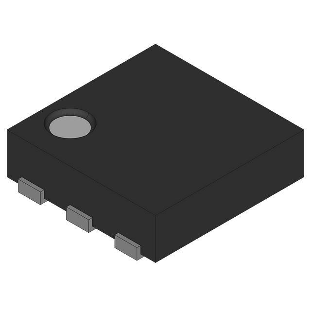
EVAL-AD5338RDBZ
Analog Devices Inc.The AD5338R, a member of the?nanoDAC? family is a low power, dual, 10-bit buffered voltage output DAC. The device includes a 2.5 V, 2 ppm/?C internal reference (enabled by default) and a gain select pin giving a full-scale output of 2.5 V (gain = 1) or 5 V (gain = 2). The device operates from a single 2.7 V to 5.5 V supply, is guaranteed monotonic by design, and exhibits less than 0.1% FSR gain error and 1.5 mV offset error performance. The device is available in a 3 mm ? 3 mm LFCSP and a TSSOP package.The AD5338R also incorporates a power-on reset circuit and a RSTSEL pin that ensures that the DAC outputs power up to zero scale or midscale and remain there until a valid write takes place. Each part contains a per-channel power-down feature that reduces the current consumption of the device to 4 ?A at 3 V while in power-down mode.The AD5338R uses a versatile 2-wire serial interface that operates at clock rates up to 400 kHz, and includes a VLOGIC pin intended for 1.8 V/3 V/5 V logic.PRODUCT HIGHLIGHTS Excellent DC Performance: Total Unadjusted Error: ?0.1% of FSR maximum Low Drift On-Chip Reference: 2.5V, 2 ppm/?C typical temperature coefficient Two Package Options: 3 mm ? 3 mm, 16-lead LFCSP or 16-lead TSSOPAPPLICATIONS Optical transceivers Base-station power amplifiers Process control (PLC I/O cards) Industrial automation Data acquisition systems

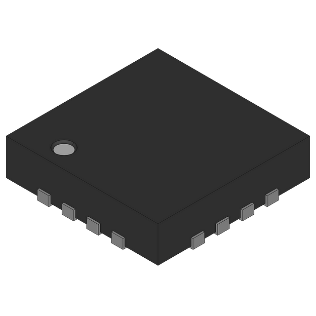
EVAL-AD5341DBZ
Analog Devices Inc.The AD5330/AD5331/AD5340/AD5341* are single 8-/10-/12-bit DACs. They operate from a 2.5 V to 5.5 V supply consuming just 115 ?A at 3 V and feature a power-down mode that further reduces the current to 80 nA. The devices incorporate an on-chip output buffer that can drive the output to both supply rails, but the AD5330, AD5340, and AD5341 allow a choice of buffered or unbuffered reference input. The AD5330/AD5331/AD5340/AD5341 have a parallel interface. CS selects the device and data is loaded into the input registers on the rising edge of WR. The GAIN pin allows the output range to be set at 0 V to VREF or 0 V to 2 ? VREF. Input data to the DACs is double-buffered, allowing simultaneous update of multiple DACs in a system using the LDAC pin. An asynchronous CLR input is also provided, which resets the contents of the input register and the DAC register to all zeros. These devices also incorporate a power-on reset circuit that ensures that the DAC output powers on to 0 V and remains there until valid data is written to the device. The AD5330/AD5331/AD5340/AD5341 are available in thin shrink small outline packages (TSSOP).ApplicationsPortable battery-powered instruments Digital gain and offset adjustment Programmable voltage and current sources Programmable attenuators Industrial process control * Protected by U.S. Patent Number 5,969,657; other patents pending. Data Sheet, Rev. A, 2/08

EVAL-AD5342DBZ
Analog Devices Inc.The AD5332?/ AD5333?/ AD5342 / AD5343?are dual 8-,10-,and 12-bit DACs. They operate from a 2.5 V to 5.5 V supply consuming just 230 ?A at 3 V, and feature a power-down pin, PD that further reduces the current to 80 nA. These devices incorporate an on-chip output buffer that can drive the output to both supply rails, while the AD5333 and AD5342 allow a choice of buffered or unbuffered reference input.PRODUCT HIGHLIGHTS Available in a 28-lead TSSOP package Low power, single supply operation from 2.5 V to 5.5 V supply Consumes 0.69 mW at 3 V and 1.5 mW at 5 V On-chip output buffer can drive output to both supply rails Allows a choice of buffered/unbuffered reference input Programmable output range 0-VREF or 0-2VREF (via GAIN pin)
EVAL-AD5343DBZ
Analog Devices Inc.The AD5332?/ AD5333?/ AD5342?/ AD5343 are dual 8-,10-,and 12-bit DACs. They operate from a 2.5 V to 5.5 V supply consuming just 230 ?A at 3 V, and feature a power-down pin, PD that further reduces the current to 80 nA. These devices incorporate an on-chip output buffer that can drive the output to both supply rails, while the AD5333 and AD5342 allow a choice of buffered or unbuffered reference input.PRODUCT HIGHLIGHTS Available in a 20-lead TSSOP package Low power, single supply operation from 2.5 V to 5.5 V supply Consumes 0.69 mW at 3 V and 1.5 mW at 5 V On-chip output buffer can drive output to both supply rails 8-Bit Parallel interface for upper and lower byte load (controlled via HBEN pin)

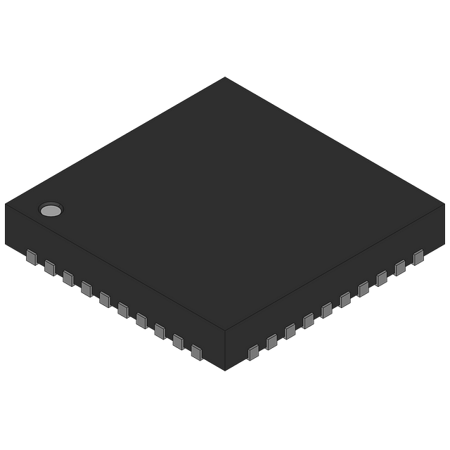
EVAL-AD5362EBZ
Analog Devices Inc.The AD5362 / AD5363 contains 8, 16/14-bit DACs in a single, 56-lead, LFCSP or 52-lead LQFP package. It provides buffered voltage outputs with a span 4 times the reference voltage. The gain and offset of each DAC can be independently trimmed to remove errors. For even greater flexibility, the device is divided into two groups of 4 DACs, and the output range of each group can be independently adjusted by an offset DAC.The AD5362 / AD5363 offers guaranteed operation over a wide supply range with VSS from -4.5 V to -16.5 V and VDD from +8 V to +16.5 V. The output amplifier headroom requirement is 1.4 V operating with a load current of 1 mA.The AD5362 / AD5363 has a high-speed serial interface, which is compatible with SPI?, QSPI?, MICROWIRE?, and DSP interface standards and can handle clock speeds of up to 50 MHz. All the outputs can be updated simultaneously by taking the LDAC input low. Each channel has a programmable gain and an offset adjust register.Each DAC output is amplified and buffered on-chip with respect to an external SIGGND input. The DAC outputs can also be switched to SIGGND via the CLR pin.APPLICATIONS Instrumentation Industrial Control System Level setting in automatic test equipment (ATE) Variable optical attenuators (VOA) Optical line cards


