
104987-HMC407MS8G
Analog Devices Inc.The HMC407MS8G & HMC407MS8GE are high?efficiency GaAs InGaP Heterojunction Bipolar?Transistor (HBT) MMIC Power amplifiers which?operate between 5 and 7 GHz. The amplifier requires?no external matching to achieve operation and is?thus truly 50 Ohm matched at input and output. The?amplifier is packaged in a low cost, surface mount?8 leaded package with an exposed base for improved?RF and thermal performance. The amplifier?provides 15 dB of gain, +29 dBm of saturated power?at 28% PAE from a +5V supply voltage. Power down?capability is available to conserve current consumption?when the amplifier is not in use.Applications UNII HiperLAN

105173-HMC415LP3
Analog Devices Inc.The HMC415LP3(E) is a high efficiency GaAs InGaP Heterojunction Bipolar Transistor (HBT) MMIC Power amplifier which operates between 4.9 and 5.9 GHz. The amplifier is packaged in a low cost, leadless surface mount package with an exposed base for improved RF and thermal performance. With a minimum of external components, the amplifier provides 20 dB of gain, +26 dBm of saturated power, and 34% PAE from a +3V supply voltage. Vpd can be used for full power down or RF output power/current control. For +15 dBm OFDM output power (64 QAM, 54 Mbps), the HMC415LP3(E) achieves an error vector magnitude (EVM) of 3.7% meeting 802.11a linearity requirements.Applications 802.11a WLAN HiperLAN WLAN Access Points UNII & ISM Radios

105706-HMC384LP4
Analog Devices Inc.The HMC384LP4(E) is a GaAs InGaP Heterojunction Bipolar Transistor (HBT) MMIC VCO with integrated resonator, negative resistance device, varactor diode, and buffer amplifier. The VCO?s phase noise performance is excellent over temperature, shock, vibration and process due to the oscillator?s monolithic structure. Power output is 3.5 dBm typical from a 3V supply voltage. The voltage controlled oscillator is packaged in a low cost leadless QFN 4x4 mm surface mount package.APPLICATIONS Wireless Infrastructure Industrial Controls Test Equipment Military

105706-HMC390LP4
Analog Devices Inc.The HMC390LP4(E) is a GaAs InGaP Heterojunction Bipolar Transistor (HBT) MMIC VCO with integrated resonator, negative resistance device, varactor diode, and buffer amplifier. Covering 3.55 to 3.9 GHz, the VCO?s phase noise performance is excellent over temperature, shock, vibration and process due to the oscillator?s monolithic structure. Power output is 4.7 dBm typical from a single supply of 3V @ 42 mA. The voltage controlled oscillator is packaged in a low cost leadless QFN 4?4 mm surface mount package.APPLICATIONS Wireless Local Loop (WLL) VSAT & Microwave Radio Test Equipment & Industrial Controls Military

105706-HMC429LP4
Analog Devices Inc.The HMC429LP4(E) is a GaAs InGaP Heterojunction Bipolar Transistor (HBT) MMIC VCO with an integrated resonator, negative resistance device, varactor diode, and buffer amplifier. Covering 4.45 to 5.0 GHz, the VCO?s phase noise performance is excellent over temperature, shock, vibration and process due to the oscillator?s monolithic structure. Power output is 4 dBm typical from a single supply of 3V @ 30mA. The voltage controlled oscillator is packaged in a low cost leadless QFN 4x4 mm surface mount package.APPLICATIONS 802.11a, HiperLAN WLAN VSAT, UNII & Microwave Radio Test Equipment & Industrial Controls Military

105706-HMC505LP4
Analog Devices Inc.The HMC505LP4(E) is a GaAs InGaP Heterojunction Bipolar Transistor (HBT) MMIC VCO with an integrated resonator, negative resistance device, varactor diode, and buffer amplifier. Covering 6.8 to 7.4 GHz, the VCO?s phase noise performance is excellent over temperature, shock and vibration due to the oscillator?s monolithic structure. Power output is +11 dBm typical from a single supply of +3V @ 80 mA. The voltage controlled oscillator is packaged in a leadless QFN 4x4 mm surface mount package.APPLICATIONS VSAT & Microwave Radio Test Equipment & Industrial Controls Military

105809-HMC439QS16G
Analog Devices Inc.The HMC439QS16G(E) is a digital phase-frequency detector intended for use in low noise phase-locked loop applications for inputs from 10 to 1300 MHz. Its combination of high frequency of operation along with its ultra low phase noise floor make possible synthesizers with wide loop bandwidth and low N resulting in fast switching and very low phase noise. When used in conjunction with a differential loop amplifier, the HMC439QS16G(E) generate output voltages that can be used to phase lock a VCO to a reference oscillator. The device is packaged in a low cost, surface mount 16 lead QSOP package with an exposed base for improved RF and thermal performance.APPLICATIONS Point-to-Point Radios Satellite Communication Systems Military Applications Sonet Clock Generation

107010-HMC472ALP4
Analog Devices Inc.The HMC472ALP4E are broadband 6-bit GaAs IC digital attenuators in low cost leadless surface mount packages. This single positive control line per bit digital attenuator incorporates off chip AC ground capacitors for near DC operation, making it suitable for a wide variety of RF and IF applications. Covering DC to 3.8 GHz, the insertion loss is less than 2.0 dB typical. The attenuator bit values are 0.5 (LSB), 1, 2, 4, 8, and 16 dB for a total attenuation of 31.5 dB. Attenuation accuracy is excellent at ? 0.25 dB typical step error with an IIP3 of +54 dBm. Six TTL/CMOS control inputs are used to select each attenuation state. A single Vdd bias of +5V is required.APPLICATIONSThe HMC472ALP4E is ideal for: 3G Infrastructure & access points? Cellular/3G, LTE & UMB WiMAX, WiBN & Fixed Wireless? Test Equipment and Sensors GSM, WCDMA & TD-SCDMA

107755-HMC454ST89
Analog Devices Inc.The HMC454ST89(E) is a high dynamic range GaAs InGaP Heterojunction Bipolar Transistor (HBT) 1?2 watt MMIC amplifier operating between 0.4 and 2.5 GHz. Packaged in a low cost industry standard SOT89, the amplifier gain is typically 17.8 dB from 0.8 to 1.0 GHz and 12.5 dB from 1.8 to 2.2 GHz. Utilizing a minimum number of external components and a single +5V supply, the amplifier output IP3 can be optimized to +40 dBm at 0.9 GHz or +42 dBm at 2.0 GHz. The high output IP3 and PAE makes the HMC454ST89(E) an ideal driver amplifier for Cellular/PCS/3G, WLL, ISM and Fixed Wireless applications.Applications GSM, GPRS & EDGE? CDMA & W-CDMA? CATV/Cable Modem? Fixed Wireless & WLL

107795-HMC356LP3
Analog Devices Inc.The HMC356LP3(E) is a high dynamic range GaAs PHEMT MMIC Low Noise Amplifier is ideal for GSM & CDMA cellular basestation and Mobile Radio front-end receivers operating between 350 and 550 MHz. This LNA has been optimized to provide 1 dB noise figure, 17 dB gain and +38 dBm output IP3 from a single supply of +5V @ 104 mA. Input and output return losses are 15 dB typical, with the LNA requiring only four external components to optimize the RF input match, RF ground and DC bias.Applications GSM 450 & GSM 480 CDMA 450 Private Land Mobile Radio

107846-HMC368LP4
Analog Devices Inc.The HMC368LP4(E) is a miniature amp-doubler-amps utilizing GaAs PHEMT technology in 4 ? 4 mm leadless surface mount package. When driven by a +2 dBm signal, the multiplier provides +15 dBm typical output power from 9 to 16 GHz. The Fo and the 3Fo isolations are 18 dB typical. The low additive SSB phase noise of ?140 dBc/Hz at 100 kHz offset helps the user maintain good system noise performance. The HMC368LP4(E) is ideal for use in LO multiplier chains allowing reduced parts count vs. traditional approaches.APPLICATIONS Microwave Radios & VSAT Fiber Optic Infrastructure Military Communications & Radar

108709-HMC453QS16G
Analog Devices Inc.The HMC453QS16G(E) is a high dynamic range GaAs InGaP Heterojunction Bipolar Transistor (HBT) 1.6 watt MMIC power amplifier operating between 0.4 and 2.2 GHz. Packaged in a miniature 16 lead QSOP plastic package, the amplifier gain is typically 21.5 dB at 0.4 GHz and 8 dB at 2.1 GHz. Utilizing a minimum number of external components and a single +5V supply, the amplifier output IP3 can be optimized to +47 dBm at 0.4 GHz or +51 dBm at 2.1 GHz. The power control (VPD) can be used for full power down or RF output power/current control. The high output IP3 and PAE make the HMC453QS16G(E) ideal power amplifier for Cellular/ PCS/3G, WLL, ISM and Fixed Wireless applications.Applications GSM, GPRS & EDGE? CDMA & W-CDMA? CATV/Cable Modem? Fixed Wireless & WLL

109258-HMC374
Analog Devices Inc.The HMC374(E) is a general purpose broad band Low Noise Amplifier (LNA) for use in the 0.3 - 3.0 GHz frequency range. The LNA provides 15 dB of gain and a 1.5 dB noise figure from a single positive supply of +2.75 to +5.5V. The low noise figure coupled with a high P1dB (22 dBm) and high OIP3 (37 dBm) make this part ideal for cellular applications. The compact LNA design utilizes on-chip matching for repeatable gain and noise figure performance. To minimize board area the design is offered in a low cost SOT26 package that occupies only 0.118? x 0.118?.Applications Cellular/PCS/3G? WCS, MMDS & ISM? Fixed Wireless & WLAN? Private Land Mobile Radio
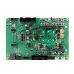
The ADuCM4050WL EZ-KIT® from Analog Devices, Inc. is an evaluation system for the ADuCM4050 processor
Analog Devices Inc.The ADuCM4050WL EZ-KIT® and ADuCM4050LF EZ-KIT®, Analog Devices, Inc. are an evaluation system for the ADuCM4050 MCU, for the WLCSP and LFCSP packages respectively.
The ADuCM4050 processor is an ultra low-power integrated mixed-signal microcontroller system for processing,
control and connectivity. The MCU system is based on the ARM Cortex-M4F processor. The MCU also has a collection
of digital peripherals, embedded SRAM and flash memory, and an analog subsystem which provides clocking,
reset, and power management capability in addition to an ADC subsystem.
The EZ-KIT contains an array of three connectors that support the ADF7xxx Wireless Transceiver series of daughterboard
products. Refer to ADF7xxx Wireless Transceiver Daughterboard Interface for more information.
The EZ-KIT contains Expansion Interface 3 (EI3) and Arduino interfaces. These interfaces provide connections for daughterboards to expand the functionality of the EZ-KIT. Refer to Expansion Interface 3 and Arduino Interface for more information.
The evaluation board is designed to be used with with the IAR, Keil or CrossCore Embedded Studio development environments for advanced application code development and debug, such as:
Create, compile, assemble, and link application programs written in C++, C, and assembly
Load, run, step, halt, and set breakpoints in application programs
Read and write data and program memory
Read and write core and peripheral registers

DC2345A
Analog Devices Inc.The LT8391 is a synchronous 4-switch buck-boost LED controller that regulates LED current from input voltage above, below, or equal to the output voltage. The proprietary peak-buck peak-boost current mode control scheme allows adjustable and synchronizable 150kHz to 650kHz fixed frequency operation, or internal ?15% triangle spread spectrum operation for low EMI. With 4V to 60V input, 0V to 60V output, and seamless low noise transitions between operation regions, the LT8391 is ideal for LED driver and battery charger applications in automotive, industrial, and battery-powered systems.The LT8391 provides both internal (up to 128:1) and external (up to 2000:1) LED current PWM dimming with a high-side PMOS switch. Two CTRL pins provide flexible 20:1 analog dimming with ?3% LED current accuracy at 100mV full scale. Fault protection is provided to detect an open or short LED condition, during which the LT8391 retries, latches off, or keeps running. Switching Frequency Max Output Power LT8391 Adjustable 150kHz - 650kHz 450W+ LT8391A 2MHz 50W+ APPLICATIONS Automotive Head Lamps/Running Lamps High Power LED Lighting

ADP5072CB-EVALZ
Analog Devices Inc.The ADP5072 is a dual, high performance dc-to-dc regulator that generates independently regulated positive and negative rails.The input voltage range of 2.85 V to 5.5 V supports a wide variety of applications. The integrated main switch in both regulators enables generation of an adjustable positive output voltage up to 35 V and a negative output voltage down to ?30 V.The ADP5072 operates at a pin selected 1.2 MHz or 2.4 MHz switching frequency. The ADP5072 can synchronize with an external oscillator from 1.0 MHz to 2.6 MHz to ease noise filtering in sensitive applications. Both regulators implement programmable slew rate control circuitry for the MOSFET driver stage to reduce electromagnetic interference (EMI). Flexible start-up sequencing is provided with the options of manual enable, simultaneous mode, positive supply first, and negative supply first.The ADP5072 includes a fixed internal or resistor programmable soft start timer to prevent inrush current at power-up.Other key safety features in the ADP5072 include overcurrent protection (OCP), overvoltage protection (OVP), thermal shutdown (TSD), and input undervoltage lockout (UVLO).The ADP5072 is available in a 20-ball WLCSP and is rated for a ?40?C to +125?C junction temperature range.Bipolar amplifiers, analog-to-digital converters (ADCs), digital-to-analog converters (DACs), and multiplexersCharge coupled device (CCD) bias suppliesOptical module suppliesRF power amplifier biasTime of flight module supplies

EV-HT-200CDAQ1
Analog Devices Inc.The AD7981 is a 16-bit, successive approximation, PulSAR? analog-to-digital converter (ADC) designed for high temperature operation. The AD7981 is capable of sample rates of up to 600 kSPS while maintaining low power consumption from a single power supply, VDD. It is a fast throughput, high accuracy, high temperature, successive approximation register (SAR) ADC, packaged in a small form factor with a versatile serial port interface (SPI).On the CNV rising edge, the AD7981 samples an analog input, IN+, between 0 V and REF with respect to a ground sense, IN?. The reference voltage, REF, is applied externally and can be set independent of the supply voltage, VDD. The device power scales linearly with throughput.The SPI-compatible serial interface also features the ability, using the SDI input, to daisy-chain several ADCs on a single, 3-wire bus and provides an optional busy indicator. It is compatible with 1.8 V, 2.5 V, 3 V, or 5 V logic, using the separate supply, VIO.For space constrained applications, the AD7981 is available in a 10-lead mini small outline package (MSOP) with operation speci-fied from ?55?C to +175?C and 10-lead ceramic flat package (FLATPACK) with operation specified from ?55?C to +210?C. These packages are designed for robustness at extreme temperatures, including monometallic wire bonding, and are qualified for up to 1000 hours of operation at the maximum temperature rating.The AD7981 is a member of a growing series of high temperature qualified products offered by Analog Devices, Inc. For a complete selection of available high temperature products, see the high temperature product list and qualification data available at www.analog.com/hightemp.Applications Oil and gas exploration Avionics Heavy industrial High temperature environments Scientific instrumentation

EVAL-AD7766EDZ
Analog Devices Inc.The AD7766/AD7766-1/AD7766-2 are high performance,24-bit, oversampled SAR analog-to-digital converters (ADCs).The AD7766/AD7766-1/AD7766-2 combine the benefits of alarge dynamic range and input bandwidth, consuming 15 mW,10.5 mW, and 8.5 mW power, respectively, and are contained ina 16-lead TSSOP package.Ideal for ultralow power data acquisition (such as PCI- and USBbasedsystems), the AD7766/AD7766-1/AD7766-2 provide 24-bitresolution. The combination of exceptional SNR, wide dynamicrange, and outstanding dc accuracy make the AD7766/AD7766-1/AD7766-2 ideally suited for measuring small signal changes over awide dynamic range. This is particularly suitable for applicationswhere small changes on the input are measured on larger ac ordc signals. In such an application, the AD7766/AD7766-1/AD7766-2 accurately gather both ac and dc information.The AD7766/AD7766-1/AD7766-2 include an on-board digitalfilter (complete with linear phase response) that acts to eliminateout-of-band noise by filtering the oversampled input voltage.The oversampled architecture also reduces front-end antialiasrequirements. Other features of the AD7766/AD7766-1/AD7766-2include a SYNC/PD (synchronization/power-down) pin, allowingthe synchronization of multiple AD7766/AD7766-1/AD7766-2devices. The addition of an SDI pin provides the option of daisychaining multiple AD7766/AD7766-1/AD7766-2 devices.The AD7766/AD7766-1/AD7766-2 operate from a 2.5 V supplyusing a 5 V reference. The devices operate from ?40?C to +105?C. Applications Low power PCI/USB data acquisition systems Low power wireless acquisition systems Vibration analysis Instrumentation High precision medical acquisition

EVAL-AD7262EDZ
Analog Devices Inc.The AD7262/AD7262-5 are dual, 12-bit, high speed, low power, successive approximation ADCs that operate from a single 5 V power supply. The AD7262 features throughput rates of up to 1 MSPS per on-chip ADC. The AD7262-5 features throughput rates of up to 500 kSPS. Two complete ADC functions allow simultaneous sampling and conversion of two channels. Each ADC is preceded by a true differential analog input with a PGA. There are 14 gain settings available: ?1, ?2, ?3, ?4, ?6, ?8, ?12, ?16, ?24, ?32, ?48, ?64, ?96, and ?128.The AD7262/AD7262-5 contain four comparators. Comparator A and Comparator B are optimized for low power, while Comparator C and Comparator D have fast propagation delays. The AD7262/AD7262-5 feature a calibration function to remove any device offset error and programmable gain adjust registers to allow for input path (for example, sensor) offset and gain compensation. The AD7262/AD7262-5 have an on-chip 2.5 V reference that can be disabled if an external reference is preferred.The AD7262/AD7262-5 are ideally suited for monitoring small amplitude signals from a variety of sensors. They include all the functionality needed for monitoring the position feedback signals from a variety of analog encoders used in motor control systems.Product Highlights Integrated PGA with a variety of flexible gain settings to allow detection and conversion of low level analog signals. Each PGA is followed by a dual simultaneous sampling ADC, featuring throughput rates of 1 MSPS per ADC for the AD7262. The conversion results of both ADCs are simultaneously available on separate data lines or in succession on one data line if only one serial port is available. Four integrated comparators that can be used to count signals from pole sensors in motor control applications. Internal 2.5 V reference.


