DC1220B
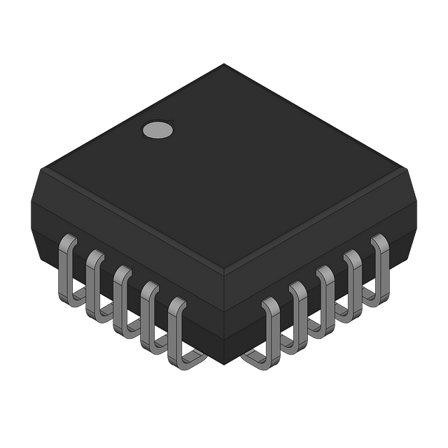
Analog Devices Inc.The LTC3225/LTC3225-1 are programmable supercapacitor chargers designed to charge two supercapacitors in series to a selectable fixed output voltage (4.8V/5.3V for the LTC3225 and 4V/4.5V for the LTC3225-1) from input supplies as low as 2.8V to 5.5V. Automatic cell balancing prevents overvoltage damage to either supercapacitor. No balancing resistors are required. Low input noise, low quiescent current and low external parts count (one flying capacitor, one bypass capacitor at VIN and one programming resistor) make the LTC3225/LTC3225-1 ideally suited for small battery-powered applications. Charge current level is programmed with an external resistor. When the input supply is removed, the LTC3225/LTC3225-1 automatically enter a low current state, drawing less than 1?A from the supercapacitors. The LTC3225/LTC3225-1 are available in a 10-lead 2mm ? 3mm DFN package.Applications Current Limited Applications with High Peak Power Loads (LED Flash, PCMCIA Tx Bursts, HDD Bursts, GPRS/GSM Transmitter) Backup Supplies

LTC3534EDHC Demo Board | 5V, 500mA Synchronous Buck-Boost DC/DC Converter
Analog Devices Inc.Demonstration Circuit 1227A is a wide VIN, high efficiency, fixed frequency synchronous Buck-Boost converter using the LTC3534EDHC. The LTC3534EDHC topology operates with input voltages above, below or equal to the output voltage, making the product ideal for multi-cell Alkaline/NiMH or single Lithium Ion/Polymer applications where the output voltage is within the battery voltage range.
The LTC3534EDHC operates with a 2.4V to 7V input voltage range and a VOUT range of 1.8V to 7V. The demonstration board has been designed to operate with VIN from 3.6V to 7V and VOUT is set to 5V with an output current up to 500mA.

DC1228A
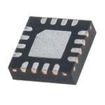
Analog Devices Inc.The LT3573 is a monolithic switching regulator specifically designed for the isolated flyback topology. No third winding or opto-isolator is required for regulation. The part senses the isolated output voltage directly from the primary-side flyback waveform. A 1.25A, 60V NPN power switch is integrated along with all control logic into a 16-lead MSOP package.The LT3573 operates with input supply voltages from 3V to 40V, and can deliver output power up to 7W with no external power devices.The LT3573 utilizes boundary mode operation to provide a small magnetic solution with improved load regulation.Applications Industrial, Automotive and Medical Isolated Power Supplies

LT5579IUH | 240MHz IF, 1.95GHz RF Upconverting Mixer Demo Board
Analog Devices Inc.DC1233A-D: Demo Board for LT5579 1.5GHz to 3.8GHz High Linearity Upconverting Mixer.

LTC6601-2 | Low Power, Low Distortion Configurable Broadband Filter Demo Board
Analog Devices Inc.DC1251A-B: Demo Board for LTC6601-2 - Low Power, Low Distortion, Low Power, Low Distortion, 5MHz to 27MHz, Pin Configurable Filter/ADC Driver

DC1255A-A
Analog Devices Inc.The LTC1605 is a 100ksps, sampling 16-bit A/D converter that draws only 55mW (typical) from a single 5V supply. This easy-to-use device includes sample-and-hold, precision reference, switched capacitor successive approximation A/D and trimmed internal clock.The LTC1605?s input range is an industry standard ?10V. Maximum DC specs include ?2.0LSB INL and 16-bits no missing codes over temperature. An external reference can be used if greater accuracy over temperature is needed.The ADC has a microprocessor compatible, 16-bit or two byte parallel output port. A convert start input and a data ready signal (BUSY) ease connections to FIFOs, DSPs and microprocessors. Input Voltage Range LTC1605 Bipolar ?10V LTC1605-1 Unipolar 0V to 4V LTC1605-2 Bipolar ?4V Applications Industrial Process Control Multiplexed Data Acquisition Systems High Speed Data Acquisition for PCs Digital Signal Processing