Manufacturer
Stock

Displaying 1 - 20 of 5422

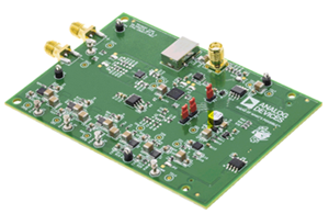
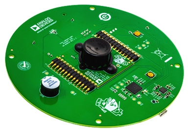
Evaluation Kits from Analog Devices Inc.

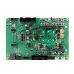
EVAL-ADG901EBZ

Analog Devices Inc.
The ADG901/ADG902 are wideband switches that use a complementary metal-oxide semiconductor (CMOS) process to provide high isolation and low insertion loss to 1 GHz. The ADG901 is an absorptive (matched) switch with 50 ? terminated shunt legs, while the ADG902 is a reflective switch. These devices are designed such that the isolation is high over the dc to 1 GHz frequency range. These switches enable the user to pass dc signals up to 0.5 V without the use of a dc blocking capacitor. They have on-board CMOS control logic, thus eliminating the need for external controlling circuitry. The control inputs are both CMOS and LVTTL compatible. The low power consumption of these CMOS devices makes them ideally suited to wireless applications and general-purpose high frequency switching.Product Highlights 40 dB Off Isolation at 1 GHz 0.8 dB Insertion Loss at 1 GHz 17 dBm P1dB at 1 GHzApplications Wireless communications General purpose RF switching Dual-band applications High speed filter selection Digital transceiver front-end switch IF switching Tuner modules Antenna diversity switching list

ADP150 Signal Chain Evaluation Board | Dual Boost/Inverting Converter

Analog Devices Inc.
Demonstration circuit SCP-ADP150-EVALZ features the ADP150, an ultralow noise (9μV), low dropout, linear regulator that operates from 2.2V to 5.5V and provides up to 150mA of output current. ADP150AUJZ-3.3-R7 fixed volt-age IC is installed on this board. Like all boards in the Signal Chain Power series, this board is designed to be easily plugged into other SCP boards to form a complete signal chain power system, enabling fast evaluation of low power signal chains. To evaluate this board, some universal SCP hardware is required, namely: SCP-INPUT-EVALZ SCP-OUTPUT-EVALZ SCP-FILTER-EVALZ SCP-THRUBRD-EVALZ SCP-1X2BKOUT-EVALZ SCP-1X5BKOUT-EVALZ SCP-5X1-EVALZ   To properly evaluate SCP series demo boards, you will need the SCP Configurator companion software. SCP Configurator can help you choose the right board and topology for your design. Note that the Demo Manual does not cover details important to the operation and configuration regarding the ADP150. Please refer to the ADP150 datasheet for a complete description of the part.

ADP5070 Signal Chain Evaluation Board | Dual Boost/Inverting Converter

Analog Devices Inc.
Demonstration circuit SCP-ADP5070-EVALZ is a dual out-put DC-DC converter designed to create a dual polarity regulated voltage for powering several signal chains. The positive regulator provides 15V/1A of output while the negative regulator delivers –15V/300mA. Like all boards in the Signal Chain Power series, this board is designed to be easily plugged into other SCP boards to form a complete signal chain power system, enabling fast evaluation of low power signal chains. To evaluate this board, some universal SCP hardware is required, namely: SCP-INPUT-EVALZ SCP-OUTPUT-EVALZ SCP-1X5BKOUT-EVALZ SCP-THRUBRD-EVALZ SCP-FILTER-EVALZ SCP-1X2BKOUT-EVALZ SCP-5X1-EVALZ   To properly evaluate SCP series demo boards, you will need the SCP Configurator companion software. SCP Configurator can help you choose the right board and topology for your design. Note that the Demo Manual does not cover details important to the operation and configuration regarding the ADP5070. Please refer to the ADP5070 datasheet for a complete description of the part.

LT1956 Signal Chain Evaluation Board | 60V/1.5A Inverting Buck Converter

Analog Devices Inc.
Demonstration circuit SCP-LT1956-IEVALZ is a 48V, 1.5A buck regulator configured as an inverting buck topology for positive to negative DC voltage conversion. This board has ample current output to drive multiple signal chains. Like all boards in the Signal Chain Power series, this board is designed to be easily plugged into other SCP boards to form a complete signal chain power system, enabling fast evaluation of low power signal chains. To evaluate this board, some universal SCP hardware is required, namely: SCP-INPUT-EVALZ SCP-OUTPUT-EVALZ SCP-1X5BKOUT-EVALZ SCP-THRUBRD-EVALZ SCP-FILTER-EVALZ SCP-1X2BKOUT-EVALZ SCP-5X1-EVALZ   To properly evaluate SCP series demo boards, you will need the SCP Configurator companion software. SCP Configurator can help you choose the right board and topology for your design. Note that this Demo Manual does not cover details important to the operation and configuration regarding the LT1956. Please refer to the LT1956 datasheet for a complete description of the part.

LT3483 Signal Chain Evaluation Board | Inverting μPower DC/DC Converter

Analog Devices Inc.
Demonstration circuit SCP-LT3483-EVALZ is an inverting converter featuring the LT3483ES6. The converter generates –15V at 8mA to 40mA from a 2.7–12V input using a dual coupled inductor in an inverting flyback topology. Like all boards in the Signal Chain Power series, this board is designed to be easily plugged into other SCP boards to form a complete signal chain power system, enabling fast evaluation of low power signal chains. To evaluate this board, some universal SCP hardware is required, namely: SCP-INPUT-EVALZ SCP-OUTPUT-EVALZ SCP-1X5BKOUT-EVALZ SCP-THRUBRD-EVALZ SCP-FILTER-EVALZ SCP-1X2BKOUT-EVALZ SCP-5X1-EVALZ   To properly evaluate SCP series demo boards, you will need the SCP Configurator companion software. SCP Configurator can help you choose the right board and to-pology for your design. Note that the Demo Manual does not cover details important to the operation and configuration regarding the LT3483 buck regulator. Please refer to the LT3483 data sheet for a complete description of the part.

LT8330 Signal Chain Evaluation Board | Boost Converter w/ 1A, 60V Switch

Analog Devices Inc.
Demonstration circuit SCP-LT8330-EVALZ features the LT8330, a boost/SEPIC/inverting converter with a 1A, 60V switch. The demo circuit is specifically a boost converter with an operating input voltage range from 10V to 36V and an output voltage of 48V. With a 12V input, the maximum output current is 135mA. Like all boards in the Signal Chain Power series, this board is designed to be easily plugged into other SCP boards to form a complete signal chain power system, enabling fast evaluation of low power signal chains. To evaluate this board, some universal SCP hardware is required, namely: SCP-INPUT-EVALZ SCP-OUTPUT-EVALZ SCP-FILTER-EVALZ SCP-THRUBRD-EVALZ SCP-1X2BKOUT-EVALZ SCP-1X5BKOUT-EVALZ SCP-5X1-EVALZ   To properly evaluate SCP series demo boards, you will need the SCP Configurator companion software. SCP Configurator can help you choose the right board and topology for your design. Note that the Demo Manual does not cover details important to the operation and configuration regarding the LT8330. Please refer to the LT8330 datasheet for a complete description of the part.

LTC3114 Signal Chain Evaluation Board | 40V, 1A Synchronous Buck-Boost DC/DC Converter with Programmable Output Current

Analog Devices Inc.
Demonstration circuit SCP-LTC3114-1-EVALZ features the LTC3114-1, a wide operating range, synchronous mono-lithic buck-boost converter with programmable average output current. The circuit operates with a 2.2V to 40V in-put voltage range. Like all boards in the Signal Chain Power series, this board is designed to be easily plugged into other SCP boards to form a complete signal chain power system, enabling fast evaluation of low power signal chains. To evaluate this board, some universal SCP hardware is required, namely: SCP-INPUT-EVALZ SCP-OUTPUT-EVALZ SCP-1X5BKOUT-EVALZ SCP-THRUBRD-EVALZ SCP-FILTER-EVALZ SCP-1X2BKOUT-EVALZ SCP-5X1-EVALZ   To properly evaluate SCP series demo boards, you will need the SCP Configurator companion software. SCP Configurator can help you choose the right board and topology for your design. Note that the Demo Manual does not cover details important to the operation and configuration regarding the LTC3114-1. Please refer to the LTC3114-1 data sheet for a complete description of the part.

EVAL-ADCMP606BKSZ

Analog Devices Inc.
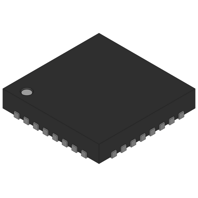
The ADCMP606 and ADCMP607 are very fast comparatorsfabricated on XFCB2, an Analog Devices, Inc., proprietaryprocess. These comparators are exceptionally versatile and easyto use. Features include an input range from VEE ? 0.5 V toVCCI + 0.2 V, low noise, CML-compatible output drivers, andTTL-/CMOS-compatible latch inputs with adjustable hysteresisand/or shutdown inputs.The devices offer 1.25 ns propagation delay with 2.5 ps rmsrandom jitter (RJ). Overdrive and slew rate dispersion aretypically less than 50 ps.A flexible power supply scheme allows the devices to operatewith a single +2.5 V positive supply and a ?0.5 V to +2.7 Vinput signal range up to a +5.5 V positive supply with a ?0.5 Vto +5.7 V input signal range. The ADCMP607 features splitinput/output supplies with no sequencing restrictions tosupport a wide input signal range with independent outputswing control and power savings.The CML-compatible output stage is fully back-matched forsuperior performance. The comparator input stage offers robustprotection against large input overdrive, and the outputs do notphase reverse when the valid input signal range is exceeded. Onthe ADCMP607, latch and programmable hysteresis features arealso provided with a unique single-pin control option.The ADCMP606 is available in a 6-lead SC70 package and theADCMP607 is available in a 12-lead LFCSP package.Applications High speed instrumentation Clock and data signal restoration Logic level shifting or translation Pulse spectroscopy High speed line receivers Threshold detection Peak and zero-crossing detectors High speed trigger circuitry Pulse-width modulators Current-/voltage-controlled oscillators Automatic test equipment (ATE)

EVAL-AD7705EBZ

Analog Devices Inc.
The AD7705 / AD7706?are complete analog front ends for low frequency measurement applications. These 2-/3-channel devices can accept low level input signals directly from a transducer and produce serial digital output. The devices employ a ?-? conversion technique to realize up to 16 bits of no missing codes performance. The selected input signal is applied to a proprietary, programmable-gain front end based around an analog modulator. The modulator output is processed by an on-chip digital filter. The first notch of this digital filter can be programmed via an on-chip control register, allowing adjustment of the filter cutoff and output update rate. The AD7705 / AD7706 devices operate from a single 2.7 V to 3.3 V or 4.75 V to 5.25 V supply. The AD7705 features two fully differential analog input channels; the AD7706 features three pseudo differential input channels. Both devices feature a differential reference input. Input signal ranges of 0 mV to 20 mV through 0 V to 2.5 V can be incorporated on both devices when operating with a VDD of 5 V and a reference of 2.5 V. They can also handle bipolar input signal ranges of ?20 mV through ?2.5 V, which are referenced to the AIN(?) inputs on the AD7705 and to the COMMON input on the AD7706.The AD7705 / AD7706 devices, with a 3 V supply and a 1.225 V reference, can handle unipolar input signal ranges of 0 mV to 10 mV through 0 V to 1.225 V. The devices can accept bipolar input ranges of ?10 mV through ?1.225 V. Therefore, the AD7705 / AD7706 devices perform all signal conditioning and conversion for a 2-channel or 3-channel system. The AD7705 / AD7706 are ideal for use in smart, microcontroller, or DSP-based systems. The devices feature a serial interface that can be configured for 3-wire operation. Gain settings, signal polarity, and update rate selection can be configured in software using the input serial port. The parts contains self-calibration and system calibration options to eliminate gain and offset errors on the part itself or in the system. CMOS construction ensures very low power dissipation, and the power-down mode reduces the standby power consumption to 20 ?W typ. These parts are available in a 16-lead, wide body (0.3 inch), plastic dual in-line package (DIP); a 16-lead, wide body (0.3 inch), standard small outline (SOIC) package; and a low profile, 16-lead, thin shrink small outline package (TSSOP).

119394-HMC639ST89

Analog Devices Inc.
The HMC639ST89(E) is a GaAs PHEMT, High Linearity, Low Noise, Wideband Gain Block Amplifier covering 0.2 to 4.0 GHz. Packaged in an industry standard SOT89, the amplifier can be used as either a cascadable 50 Ohm gain stage, a PA Pre-Driver, a Low Noise Amplifier, or a Gain Block with up to +22 dBm output power. This versatile Gain Block Amplifier is powered from a single +5V supply and requires no external matching components. The internally matched topology permits this amplifier to be readily ported between virtually any printed circuit board material, regardless of its dielectric constant, thickness, or composition.Applications Cellular / PCS / 3G WiMAX, WiBro, & Fixed Wireless CATV & Cable Modem Microwave Radio IF and RF Sections?

122329-HMC701LP6CE

Analog Devices Inc.
The HMC701LP6CE is a SiGe BiCMOS fractional-N frequency synthesizer. The synthesizer includes a 8GHz 16-bit RF N-Divider, a 24-bit delta-sigma modulator, a very low noise digital phase frequency detector (PFD), and a precision controlled charge pump. In addition the synthesizer supports an external step tuned VCO.The fractional synthesizer features an advanced delta-sigma modulator design that allows ultra-fine frequency step sizes. The synthesizer features the ability to alter both the phase-frequency detector (PFD) gain and the cycle slipping characteristics of the PFD. This feature can reduce the time to arrive at the new frequency by 50% vs. conventional PFDs. Ultra low in-close phase noise also allows wider loop bandwidths for faster frequency hopping.The synthesizer contains a built-in linear sweeper function, which allows it to perform frequency chirps with a wide variety of sweep times, polarities and dwells, all with an external or automatic sweep trigger.A General Purpose Output (GPO) bus supports the use of multiple VCOs. In addition the synthesizer has a number of auxiliary clock generation modes that can be accessed via the GPO.Applications Base Stations for Mobile Radio (GSM, PCS, DCS, CDMA, WCDMA) Wireless LANs, WiMax Communications Test Equipment CATV Equipment FMCW Sensors Automotive Radar Phased-Array Systems

123794-HMC752LC4

Analog Devices Inc.
The HMC752LC4 is a GaAs MMIC Low Noise WidebandAmplifier housed in a leadless 4x4 mm ceramicsurface mount package. The amplifier operates between24 and 28 GHz, providing up to 25 dB of smallsignal gain, 2.5 dB noise figure, and output IP3 of+26 dBm, while requiring only 70 mA from a +3V supply.The P1dB output power of up to +13 dBm enablesthe LNA to function as a LO driver for balanced, I/Qor image reject mixers. The HMC752LC4 also featuresI/Os that are DC blocked and internally matched to50 Ohms, making it ideal for high capacity microwaveradios or VSAT applications.Applications Point-to-Point Radios Point-to-Multi-Point Radios Military & Space Test Instrumentation

123987-HMC736LP4

Analog Devices Inc.
The HMC736 is a GaAs InGaP Heterojunction Bipolar Transistor (HBT) MMIC VCO. The HMC736 integrates a resonator, negative resistance device, varactor diode and feature half frequency output. The VCO's phase noise performance is excellent over temperature, shock, and process due to the oscillator's monolithic structure. Power output is +9 dBm typical from a +4.2V supply voltage. The voltage controlled oscillator is packaged in a leadless QFN 4?4 mm surface mount package, and requires no external matching components.APPLICATIONS Point-to-Multi-Point Radios Test Equipment & Industrial Controls SATCOM Military End-Use

127826-HMC821LP6CE

Analog Devices Inc.
The HMC821LP6CE is a fully functioned Fractional-N Phase-Locked-Loop (PLL) Frequency Synthesizer with an Integrated Voltage Controlled Oscillator (VCO). The synthesizer consists of an integrated low noise VCO with a triband output, an autocalibration subsystem for low voltage VCO tuning, a very low noise digital Phase Detector (PD), a precision controlled charge pump, a low noise reference path divider and a fractional divider.The fractional synthesizer features an advanced delta-sigma modulator design that allows both ultra-fine step sizes and low spurious products. The phase detector (PD) features cycle slip prevention (CSP) technology to allow faster frequency hopping times. Ultra low in-close phase noise and low spurious also allows wider loop bandwidths for faster frequency hopping and low micro-phonics.For theory of operation and register map refer to the 'PLLs with Integrated VCO - RF VCOs' Operating Guide.Applications Cellular/4G Infrastructure Repeaters and Femtocells Communications Test Equipment CATV Equipment Phased Array Applications DDS Replacement? Very High Data Rate Radios

130371-HMC778LP6CE

Analog Devices Inc.
The HMC778LP6CE is a fully functioned Fractional-N Phase-Locked-Loop (PLL) Frequency Synthesizer with an integrated Voltage Controlled Oscillator (VCO). The input reference frequency range is DC to 350 MHz while the advanced delta-sigma modulator design in the fractional synthesizer allows both ultra-fine step sizes and very low spurious products. The highly integrated structure provides excellent phase noise performance over temperature, shock and process. In addition, the HMC778LP6CE offers frequency sweep and modulation features, external triggering, double-buffering, exact frequency control, phase modulation and more. The HMC778LP6CE is packaged in a leadless QFN 6 x 6 mm surface mount package.For theory of operation and register map refer to the 'PLLs w/ Integrated VCO - Microwave VCOs' Operating Guide.Applications VSAT Radio Microwave Point-To-Point Radios Test Equipment & Industrial Control Military End-Use Phased Array Applications FMCW Radar Systems

130521-HMC900LP5E

Analog Devices Inc.
The HMC900LP5E is a 6th order, programmable bandwidth, fully calibrated, dual low pass filter. It features 0 or 10 dB input gain setting and supports arbitrary bandwidths from 3.5 to 50 MHz, and when calibrated, is accurate to ?2.5% of the desired bandwidth. It includes a filter bypass option with a bandwidth of 100 MHz, while retaining gain and common mode settings.Housed in a compact 5x5mm SMT QFN package, the HMC900LP5E requires minimal external components and provides a low cost alternative to more complicated switched discrete filter architectures. Filter calibration for the HMC900LP5E is accomplished with any reference clock rate from 20 to 80 MHz. One time programmable (OTP) memory offers unsurpassed flexibility allowing the user 'set and forget' parameters like gain, and bandwidth setting.Matched filter paths provide excellent quadrature balance, making the HMC900LP5E ideal for I/Q communications applications. The 6th order Butterworth transfer function delivers superior stop band rejection while maintaining both a flat passband and minimal group delay variation.Applications Baseband Filtering for A/D or?D/A Converters? Point-to-Point, Fixed Wireless &?Cellular Base Station Transceivers Integrated Direct Conversion Receiver (DCR)? Software Defined Radio Applications Test & Measurement Equipment

131656-HMC966LP4E

Analog Devices Inc.
The HMC966LP4E is a compact GaAs MMIC I/Q downconverter in a leadless RoHS compliant SM T package. This device provides a small signal conversion gain of 12 dB with a noise figure of 2.5 dB and 40 dBc of image rejection across the frequency band. The HMC966LP4E utilizes an LNA followed by an image reject mixer which is driven by an active x2 multiplier. The image reject mixer eliminates the need for a filter following the LNA, and removes thermal noise at the image frequency. I and Q mixer outputs are provided and an external 90? hybrid is needed to select the required sideband. The HMC966LP4E is a much smaller alternative to hybrid style image reject mixer downconverter assemblies, and is compatible with surface mount manufacturing techniques.Applications Point-to-Point &?Point-to-Multi-Point Radio Military Radar, EW & ELINT Satellite Communications

132036-HMC858LC4B

Analog Devices Inc.
The HMC858LC4B is a 2:1 Selector designed to sup-port data transmission rates of up to 14 Gbps, and selector port operation of up to 14 GHz. The selector routes one of the two differential inputs to the differential output upon assertion of the proper select port. The HMC858LC4B also features an output level control pin, VR, which allows for loss compensation or for signal level optimization.All differential input signals to the HMC858LC4B are terminated with 50 ohms to ground on-chip, and may be either AC or DC coupled. The outputs of the HMC858LC4B may be operated either differentially or single-ended. Outputs can be connected directly to a 50 ohm terminated system, while DC blocking capacitors may be used if the terminating system is 50 ohms to a non-ground DC voltage. The HMC858LC4B operates from a single -3.3V DC supply and is available in a ceramic RoHS-compliant, 4?4 mm SMT package.APPLICATIONS 2:1 Multiplexer up to 14 Gbps 16G Fiber Channel Serial Data Transmission?up to 14 Gbps Redundant Path Switching Built-in Test Broadband Test & Measurement

AD633-EVALZ

Analog Devices Inc.
The AD633 is a functionally complete, four-quadrant, analog multiplier. It includes high impedance, differential X and Y inputs, and a high impedance summing input (Z). The low impedance output voltage is a nominal 10 V full scale provided by a buried Zener. The AD633 is the first product to offer these features in modestly priced 8-lead PDIP and SOIC packages.The AD633 is laser calibrated to a guaranteed total accuracy of 2% of full scale. Nonlinearity for the Y input is typically less than 0.1% and noise referred to the output is typically less than 100 ?V rms in a 10 Hz to 10 kHz bandwidth. A 1 MHz bandwidth, 20 V/?s slew rate, and the ability to drive capacitive loads make the AD633 useful in a wide variety of applications where simplicity and cost are key concerns.The versatility of the AD633 is not compromised by its simplicity. The Z input provides access to the output buffer amplifier, enabling the user to sum the outputs of two or more multipliers, increase the multiplier gain, convert the output voltage to a current, and configure a variety of applications.The AD633 is available in 8-lead PDIP and SOIC packages. It is specified to operate over the 0?C to 70?C commercial temperature range (J Grade) or the ?40?C to +85?C industrial temperature range (A Grade).Product Highlights The AD633 is a complete four-quadrant multiplier offered in low cost 8-lead SOIC and PDIP packages. The result is a product that is cost effective and easy to apply. No external components or expensive user calibration are required to apply the AD633. Monolithic construction and laser calibration make the device stable and reliable. High (10 M?) input resistances make signal source loading negligible. Power supply voltages can range from ?8 V to ?18 V. The internal scaling voltage is generated by a stable Zener diode; multiplier accuracy is essentially supply insensitive.Applications Multiplication, division, squaring Modulation/demodulation, phase detection Voltage-controlled amplifiers/attenuators/filters

AD6672-250EBZ

Analog Devices Inc.
The AD6672 is an 11-bit intermediate receiver with sampling speeds of up to 250 MSPS. The AD6672 is designed to support communications applications, where low cost, small size, wide bandwidth, and versatility are desired.The ADC core features a multistage, differential pipelined architecture with integrated output error correction logic. The ADC features wide bandwidth inputs supporting a variety of user-selectable input ranges. An integrated voltage reference eases design considerations. A duty cycle stabilizer is provided to compensate for variations in the ADC clock duty cycle, allowing the converters to maintain excellent performance.The ADC core output is connected internally to a noise shaping requantizer (NSR) block. The device supports two output modes that are selectable via the serial port interface (SPI). With the NSR feature enabled, the outputs of the ADCs are processed such that the AD6672 supports enhanced SNR performance within a limited region of the Nyquist bandwidth while maintaining an 11-bit output resolution. The NSR block is programmed to provide a bandwidth of up to 33% of the sample clock. For example, with a sample clock rate of 250 MSPS, the AD6672 can achieve up to 73.6 dBFS SNR for an 82 MHz bandwidth at 185 MHz fIN.With the NSR block disabled, the ADC data is provided directly to the output with an output resolution of 11 bits. The AD6672 can achieve up to 66.6 dBFS SNR for the entire Nyquist bandwidth when operated in this mode. APPLICATIONS Communications Diversity radio and smart antenna (MIMO) systems Multimode digital receivers (3G) WCDMA, LTE, CDMA2000 WiMAX, TD-SCDMA I/Q demodulation systems General-purpose software radios

Displaying 1 - 20 of 5422

Latest Parts

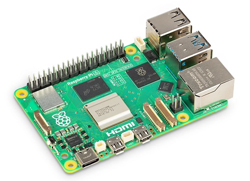
SC1112

Raspberry Pi

$79.61 - $86.40

IN STOCK 10294
Buy

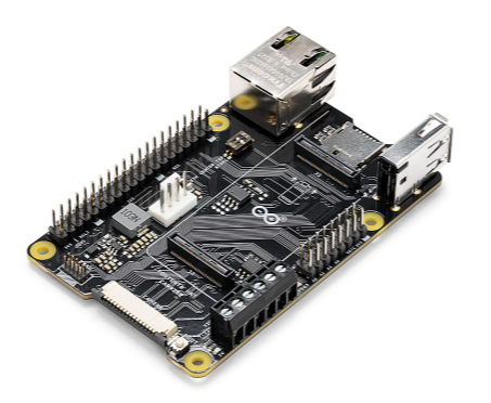
ASX00049

Arduino

* $39.45 - * $44.37

IN STOCK 3132
Buy

AD96685BRZ

Analog Devices Inc.

$1.72 - * $11.78

IN STOCK 4921
Buy

Reference Designs

RD006

Wurth Elektronik

RD006 - 3 W Dual-output isolated auxiliary supply for communication interfaces and measurement systems

CN0583

Analog Devices Inc.

Multistandard Micropower Verified Smoke Detection System-on-Module

Technical Resources

EVALUATION KITS

EVAL-AD7124-8SDZ

Analog Devices Inc.

$73.86 - * $75.91

IN STOCK 808
Buy
View All