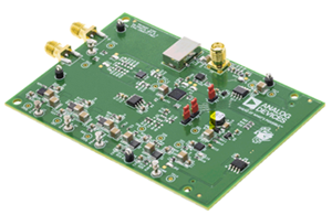
DC2367A
Analog Devices Inc.The LTM4632 is an ultrathin triple output step-down ?Module? (power module) regulator to provide complete power solution for DDR-QDR4 SRAM. Operating from a 3.6V to 15V input voltage, the LTM4632 supports two ?3A output rails, both sink and source capable, for VDDQ and VTT, plus a 10mA low noise reference VTTR output. Both VTT and VTTR track and are equal to VDDQ/2. Housed in a 6.25mm ? 6.25mm ? 1.82mm LGA and 6.25mm ? 6.25mm ? 2.42mm BGA packages, the LTM4632 includes the switching controller, power FETs, inductors and support components. Alternatively, the power module can also be configured as a two phase single ?6A output VTT. Only a few ceramic input and output capacitors are needed to complete the design.The LTM4632 supports selectable Burst Mode operation (CH1 only) and output voltage tracking for supply rail sequencing. Its high switching frequency and current mode control enable a very fast transient response to line and load changes without sacrificing stability.Fault protection features include overvoltage input, overcurrent and overtemperature protection.The LTM4632 is RoHS compliant with Pb-free finish.Applications DDR Memory Power Supply General Purpose Point of Load Conversion Telecom, Networking and Industrial Equipment
LTC1628CG-PG | High Efficiency, Multi-Phase 2-Output, Current Mode Controller, 5-30 VIN, 5V/4A and 3.3V/4A Output
Analog Devices Inc.DC236C-C: Demo Board for the LTC1628 High Efficiency, 2-Phase Synchronous Step-Down Switching Regulator.
DC2395A-F
Analog Devices Inc.The LTC2325-14 is a low noise, high speed quad 14-bit + sign successive approximation register (SAR) ADC with differential inputs and wide input common mode range. Operating from a single 3.3V or 5V supply, the LTC2325-14 has an 8VP-P differential input range, making it ideal for applications which require a wide dynamic range with high common mode rejection. The LTC2325-14 achieves ?1LSB INL typical, no missing codes at 14 bits and 81dB SNR.The LTC2325-14 has an onboard low drift (20ppm/?C max) 2.048V or 4.096V temperature-compensated reference. The LTC2325-14 also has a high speed SPI-compatible serial interface that supports CMOS or LVDS. The fast 5Msps per channel throughput with one cycle latency makes the LTC2325-14 ideally suited for a wide variety of high speed applications. The LTC2325-14 dissipates only 45mW per channel and offers nap and sleep modes to reduce the power consumption to 26?W for further power savings during inactive periods.Applications High Speed Data Acquisition Systems Communications Optical Networking Multiphase Motor Control
DC2395A-G
Analog Devices Inc.The LTC2320-12 is a low noise, high speed octal 12?bit + sign successive approximation register (SAR) ADC with differential inputs and wide input common mode range. Operating from a single 3.3V or 5V supply, the LTC2320?12 has an 8VP-P differential input range, making it ideal for applications which require a wide dynamic range with high common mode rejection. The LTC2320-12 achieves ?0.25LSB INL typical, no missing codes at 12 bits and 77dB SNR.The LTC2320-12 has an onboard low drift (20ppm/?C max) 2.048V or 4.096V temperature-compensated reference. The LTC2320-12 also has a high speed SPI-compatible serial interface that supports CMOS or LVDS. The fast 1.5Msps per channel throughput with no latency makes the LTC2320-12 ideally suited for a wide variety of high speed applications. The LTC2320-12 dissipates only 20mW per channel and offers nap and sleep modes to reduce the power consumption to 26?W for further power savings during inactive periods.Applications High Speed Data Acquisition Systems Communications Remote Data Acquisition Imaging Optical Networking Automotive Multiphase Motor Control
DC2398A
Analog Devices Inc.The LTC6373 is a precision instrumentation amplifier with fully differential outputs which includes a closely matched internal resistor network to achieve excellentCMRR, offset voltage, gain error, gain drift, and gain nonlinearity. The user can easily program the gain to one of seven available settings through a 3-bit parallel interface(A2 to A0). The 8th state puts the part in shutdown which reduces the current consumption to 220?A. Unlike a conventional voltage feedback amplifier, the LTC6373maintains nearly the same bandwidth across all its gain settings.The LTC6373 features fully differential outputs to drive high performance, differential-input ADCs. The output common mode voltage is independently adjustable viathe VOCM pin. The combination of high impedance inputs, DC precision, low noise, low distortion, and high-speed differential ADC drive makes the LTC6373 an ideal candidate for optimizing data acquisition systems.The LTC6373 is available in a 12-lead 4mm ? 4mm DFN (LFCSP) package and is fully specified over the ?40?C to 125?C temperature range.Applications Data Acquisition Systems Biomedical Instrumentation Test and Measurement Equipment Differential ADC Drivers Single-Ended-to-Differential Conversion Multiplexed Applications
DC2407A
Analog Devices Inc.The LT8650S is a dual step-down regulator that delivers up to 4A of continuous current from both channels and supports loads up to 6A from each channel. The LT8650S features the second generation Silent Switcher architecture to minimize EMI emissions while delivering high efficiency at high switching frequencies. This includes integration of bypass capacitors to optimize high frequency current loops and make it easy to achieve advertised EMI performance by eliminating layout sensitivity.The fast, clean, low-overshoot switching edges enable high efficiency operation even at high switching frequencies, leading to a small overall solution size. Peak current mode control with a 40ns minimum on-time allows high step down ratios at high switching frequencies.Burst Mode operation features a 6.2?A quiescent current resulting in high efficiency at low output currents, forced continuous mode allows fixed switching frequency operation over the entire output load range, and spread spectrum operation can further reduce EMI emissions. External VC pins allow optimal loop compensation for fast transient response. The VC pins can also be used for current sharing and the CLKOUT pin enables synchronizing two LT8650S chips to generate a 4-phase, 16A supply.APPLICATIONS General Purpose Step-Down Automotive and Industrial Supplies
DC2412A-A
Analog Devices Inc.The LTC2335-18 is an 18-bit, low noise 8-channel multiplexed successive approximation register (SAR) ADC with differential, wide common mode range inputs. Operating from a 5V low voltage supply, flexible high voltage supplies, and using the internal reference and buffer, this SoftSpan? ADC can be configured on a conversion-by-conversion basis to accept ?10.24V, 0V to 10.24V, ?5.12V, or 0V to 5.12V signals on any channel. Alternately, the ADC may be programmed to cycle through a sequence of channels and ranges without further user intervention.The wide input common mode range and 118dB CMRR of the LTC2335-18 analog inputs allow the ADC to directly digitize a variety of signals, simplifying signal chain design. This input signal flexibility, combined with ?3LSB INL, no missing codes at 18 bits, and 96.7dB SNR, makes the LTC2335-18 an ideal choice for many high voltage applications requiring wide dynamic range.The LTC2335-18 supports pin-selectable SPI CMOS (1.8V to 5V) and LVDS serial interfaces.Applications Programmable Logic Controllers Industrial Process Control Power Line Monitoring Test and Measurement
DC2414A
Analog Devices Inc.The LTC6268/LTC6269 is a single/dual 500MHz FET-input operational amplifier with extremely low input bias current and low input capacitance. It also features low input-referred current noise and voltage noise making it an ideal choice for high speed transimpedance amplifiers, CCD output buffers, and high-impedance sensor amplifiers. Its low distortion makes the LTC6268/LTC6269 an ideal amplifier for driving SAR ADCs.It operates on 3.1V to 5.25V supply and consumes 16.5mA per amplifier. A shutdown feature can be used to lower power consumption when the amplifier is not in use.The LTC6268 single op amp is available in 8-lead SOIC and 6-lead SOT-23 packages. The SOIC package includes two unconnected pins which can be used to create an input pin guard ring to protect against board leakage currents. The LTC6269 dual op amp is available in 8-lead MSOP with exposed pad and 3mm ? 3mm 10-lead DFN packages. They are fully specified over the ?40?C to 85?C and the ?40?C to 125?C temperature ranges.Applications Trans-Impedance Amplifiers ADC Drivers CCD Output Buffer Photomultiplier Tube Post-Amplifier Low IBIAS Circuits
LTM8003 Demo Board | Low EMI Buck μModule Regulator, 6V ≤ VIN ≤ 40V, VOUT = 5V @ 3.5A
Analog Devices Inc.Demonstration circuit 2416A features the LTM8003, a 40V, 3.5A step-down μModule® Regulator. This demo circuit is configured to deliver a 5.0V output from an input voltage between 6.0V to 40V at a switching frequency of 2MHz. The wide input range of the LTM8003 allows a variety of input sources such as automotive batteries and industrial supplies. Under light load conditions, the available Burst Mode® operation supports high efficiency with low output ripple.
DC2417A-B
Analog Devices Inc.The LTC4367 protects applications where power supply input voltages may be too high, too low or even negative. It does this by controlling the gate voltages of a pair of external N-channel MOSFETs to ensure that the output stays within a safe operating range.The LTC4367 withstands voltages between ?40V and 100V and has an operating range of 2.5V to 60V, while consuming only 70?A in normal operation.Two comparator inputs allow configuration of the overvoltage (OV) and undervoltage (UV) set points using an external resistive divider. A shutdown pin provides external control for enabling and disabling the MOSFETs as well as placing the device in a low current shutdown state. A fault output indicates that the GATE pin is pulling low when the part is in shutdown or the input voltage is outside the UV and OV set points.The LTC4367 has a 32ms turn-on delay that debounces live connections and blocks 50Hz to 60Hz AC power. For fast recovery after faults, the LTC4367-1 has a reduced turn-on delay of 500?s.Applications Portable InstrumentationIndustrial AutomationAutomotive Surge (Load Dump) ProtectionNetwork Equipment
LTC3372EUK#PBF Demo Board | 6V ≤ VIN ≤ 60V, VOUT_HV = 5V or 3.3V @ 10A; VOUT1 =1.2V @2A, VOUT2 =1.8V @2A, VOUT3 =2.5V @2A, VOUT4 =3.3V @2A
Analog Devices Inc.Demonstration circuit 2419A features the LTC3372 in a
multi-output step-down converter. The controller portion
of the LTC3372 drives a high output voltage (HV) buck
converter which has an input voltage range of 6V to 60V.
Its output voltage (VOUT_HV) is nominally 5V but can be
configured for either 5V or 3.3V with the VOUTPRG pin.
VOUT_HV supplies power to the configurable buck regulator.
This regulator provides four low voltage (LV) outputs
labelled VOUT1-4. These outputs are 1.2V/2A, 1.8V/2A,
2.5V/2A and 3.3V/2A respectively. When VOUT_HV is configured
for 5V, it can supply 6A to the external loads with
full load on VOUT1-4. With no load on VOUT1-4, VOUT_HV
can supply 10A to the external loads.
The LV buck regulator consists of eight power stages that
can be arranged in up to four channels. The LV regulator
on the DC2419A is setup for four channels of two power
stages each. With modifications, the LV buck regulator
can be setup for eight different configurations.
If VOUT_HV is programmed for 3.3V, then VOUT4 which
provides 3.3V/2A will be in dropout. This rail will require
an external input voltage to stay in regulation.
The LV rails operate at 2MHz and the HV converter operates
at one-sixth this frequency or 333kHz. The high frequency
of the LV rails allows the use of 4mm × 4mm
inductors. The power stage for the HV converter consists
of 60V avalanche rated MOSFETs and a 2.2μH 10mm ×
10mm inductor. A 4mΩ discrete sense resistor is used
to sense current.
The low IQ current of the LTC3372 provides high efficiency
at light loads. When the VOUT_HV is supplying the nominal
5V, its Burst Mode® efficiency with 1mA load is 90.3% for
a 12V input. When the HV converter is off,
it only draws 27μA from a 12V input.
The LTC3372 data sheet provides a complete description
of the IC operation and application information. The data
sheet must be read in conjunction with the quick start
guide.
DC2425A-A
Analog Devices Inc.The LTC2311-16 is a low noise, high speed 16-bit successive approximation register (SAR) ADC with differential inputs and wide input common mode range. Operating from a single 3.3V or 5V supply, the LTC2311- 16 has an 8VP-P differential input range, making it ideal for applications which require a wide dynamic range with high common mode rejection. The LTC2311-16 achieves ?3LSB INL typical, no missing codes at 16 bits and 81dB SNR typical.The LTC2311-16 has an onboard low drift (20ppm/?C max) 2.048V or 4.096V temperature-compensated reference and provides an external 1.25V buffered reference input. The LTC2311-16 also has a high speed SPI-compatible serial interface that supports CMOS or LVDS. The fast 5Msps throughput with one-cycle latency makes the LTC2311-16 ideally suited for a wide variety of high speed applications. The LTC2311-16 dissipates only 50mW with a 5V supply and offers nap and sleep modes to reduce the power consumption to 5?W for further power savings during inactive periods.Applications High Speed Data Acquisition Systems Communications Remote Data Acquisition Imaging Optical Networking Automotive Multiphase Motor Control
DC2425A-B
Analog Devices Inc.The LTC2310-16 is a low noise, high speed 16-bit successive approximation register (SAR) ADC with differential inputs and wide input common mode range. Operating from a single 3.3V or 5V supply, the LTC2310-16 has an 8VP-P differential input range, making it ideal for applications which require a wide dynamic range with high common mode rejection. The LTC2310-16 achieves ?3LSB INL typical, no missing codes at 16 bits and 82dB SNR typical.The LTC2310-16 has an on-board low drift (20ppm/?C max) 2.048V or 4.096V temperature-compensated reference and provides an external 1.25V buffered reference input. The LTC2310-16 also has a high speed SPI-compatible serial interface that supports CMOS or LVDS. The fast 2Msps throughput with no cycle latency makes the LTC2310-16 ideally suited for a wide variety of high speed applications. The LTC2310-16 dissipates only 35mW with a 5V supply and offers nap and sleep modes to reduce the power consumption for further power savings during inactive periods.Applications High Speed Data Acquisition Systems Communications Remote Data Acquisition Imaging Optical Networking Automotive Multiphase Motor Control
DC2425A-F
Analog Devices Inc.The LTC2310-12 is a low noise, high speed 12-bit + sign successive approximation register (SAR) ADC with differential inputs and wide input common mode range. Operating from a single 3.3V or 5V supply, the LTC2310-12 has an 8VP-P differential input range, making it ideal for applications which require a wide dynamic range with high common mode rejection. The LTC2310-12 achieves ?1LSB INL guaranteed, no missing codes at 12 bits and 73dB SNR typical.The LTC2310-12 has an onboard low drift (20ppm/?C max) 2.048V or 4.096V temperature-compensated reference and provides an external 1.25V buffered reference input. The LTC2310-12 also has a high speed SPI-compatible serial interface that supports CMOS or LVDS. The fast 2Msps throughput with no cycle latency makes the LTC2310-12 ideally suited for a wide variety of high speed applications. The LTC2310-12 dissipates only 35mW with a 5V supply and offers nap and sleep modes to reduce the power consumption for further power savings during inactive periods.Applications High Speed Data Acquisition Systems Communications Remote Data Acquisition Imaging Optical Networking Automotive Multiphase Motor Control
DC2434A
Analog Devices Inc.The LTC3864 is a robust, high voltage step-down DC/DC controller optimized for automotive and industrial applications. It drives a P-channel power MOSFET switch allowing 100% duty cycle operation. The wide input and output voltage ranges cover a multitude of applications. This device has been verified with the failure mode and effects analysis (FMEA) procedure for operation during failure conditions.The LTC3864 offers excellent light load efficiency, drawing only 40?A quiescent current in a user programmable Burst Mode operation. Its peak current mode, constant frequency PWM architecture provides for good control of switching frequency and output current limit. The switching frequency can be programmed from 50kHz to 850kHz with an external resistor and can be synchronized to an external clock from 75kHz to 750kHz.The LTC3864 offers programmable soft-start or output tracking. Safety features include overvoltage protection, overcurrent and short-circuit protection including frequency foldback and a power good output signal.The LTC3864 is available in thermally enhanced 12-Pin MSOP and 3mm ? 4mm DFN packages.Applications Industrial and Automotive Power Supplies Telecom Power Supplies Distributed Power Systems
DC2443A
Analog Devices Inc.The LT6375 is a unity-gain difference amplifier which combines excellent DC precision, a very high input common mode range and a wide supply voltage range. It includes a precision op amp and a highly-matched thin film resistor network. It features excellent CMRR, extremely low gain error and extremely low gain drift.Comparing the LT6375 to existing difference amplifiers with high common mode voltage range, the selectable resistor divider ratios of the LT6375 offer superior system performance by allowing the user to achieve maximum SNR, precision and speed for a specific input common mode voltage range.The op amp at the core of the LT6375 has Over-The-Top? protected inputs which allow for robust operation in environments with unpredictable voltage conditions. See the Applications Information section for more details.The LT6375 is specified over the ?40?C to 125?C temperature range and is available in space-saving MSOP16 and DFN14 packages.Applications High Side or Low Side Current Sensing Bidirectional Wide Common Mode Range Current Sensing High Voltage to Low Voltage Level Translation Precision Difference Amplifier Industrial Data-Acquisition Front-Ends Replacement for Isolation Circuits
LTM4636-1PolyPhase 160A Step-Down Power µModule Regulator with Overvoltage and Overtemperature Protection
Analog Devices Inc.Demonstration circuit DC2448A-D features a PolyPhase® design using the LTM4636-1EY, a 40A high efficiency, switch mode step-down power µModule® regulator with
overvoltage and overtemperature protection features. The input voltage range is from 9V to 15V. The output voltage range is 0.6V to 3.3V. The DC2448A-D can deliver a
nominal 160A output current. DC2448A-D has on-boardhot swap circuit that can disconnect input supply and protect the LTM4636-1 and the load under overvoltage and overtemperature conditions. As explained in the data sheet, output current derating is necessary for certain VIN, VOUT and thermal conditions. The board operates in continuous conduction mode in heavy load conditions.
For high efficiency at low load currents, the MODE_PLLIN jumper selects pulse-skipping mode for noise sensitive applications or Burst Mode® operation in less noise sensitive applications. The MODE_PLLIN pin also allows the LTM4636-1 to synchronize to an external clock signal. DC2448A-D has the option of choosing both internal and external compensation circuits for LTM4636-1. The LTM4636-1 data sheet must be read in conjunction with this demo manual prior to working on or modifying demo circuit DC2448A-D.
DC2449A-A
Analog Devices Inc.The LT8335 is a current mode DC/DC converter capable of generating either positive or negative output voltages using a single feedback pin. It can be configured as a boost, SEPIC or inverting converter consuming as low as 6?A of quiescent current. Low ripple Burst Mode operation maintains high efficiency down to very low output currents while keeping the output ripple below 15mV in a typical application. The internally compensated current mode architecture results in stable operation over a wide range of input and output voltages. Integrated soft-start and frequency foldback functions are included to control inductor current during start-up. The 2MHz operation combined with the small 8-lead DFN package, enables low cost, area efficient solutions.Applications Industrial and Automotive Telecom Medical Diagnostic Equipment Portable Electronics
DC2455A-B
Analog Devices Inc.The LTM4650-1A/LTM4650-1B is dual 25A or single 50A output step-down ?Module? (power module) regulator with ?0.8% (LTM4650-1A) and ?1.5% (LTM4650-1B) total DC output error with ?3% transient output error. Included in the package are the switching controller, power FETs, inductors, and all supporting components. External compensation allows for fast transient response to minimize output capacitance when powering FPGAs, ASICs, and processors. With synchronized multiphase parallel current sharing, six LTM4650-1 devices can deliver up to 300A. The LTM4650-1 is offered in a 16mm ? 16mm ? 5.01 BGA package, with SnPb (BGA) or RoHS compliant terminal finish. VIN Range VOUT Range Comp DC VOUT Accy LTM4650 4.5V to 15V 0.6V to 1.8V Internal 1.5% LTM4650-1B 4.5V to 15V 0.6V to 1.8V External 1.5% LTM4650-1A 4.5V to 15V 0.6V to 1.8V External 0.8% LTM4650A 4.5V to 16V 0.6V to 5.5V Internal 1% LTM4650A-1 4.5V to 16V 0.6V to 5.5V External 1% Applications FPGA, ASIC, ?Processor Core Voltage Regulation Information, Communication Systems
DC2455A-C
Analog Devices Inc.The LTM4650-1A/LTM4650-1B is dual 25A or single 50A output step-down ?Module? (power module) regulator with ?0.8% (LTM4650-1A) and ?1.5% (LTM4650-1B) total DC output error with ?3% transient output error. Included in the package are the switching controller, power FETs, inductors, and all supporting components. External compensation allows for fast transient response to minimize output capacitance when powering FPGAs, ASICs, and processors. With synchronized multiphase parallel current sharing, six LTM4650-1 devices can deliver up to 300A. The LTM4650-1 is offered in a 16mm ? 16mm ? 5.01 BGA package, with SnPb (BGA) or RoHS compliant terminal finish. VIN Range VOUT Range Comp DC VOUT Accy LTM4650 4.5V to 15V 0.6V to 1.8V Internal 1.5% LTM4650-1B 4.5V to 15V 0.6V to 1.8V External 1.5% LTM4650-1A 4.5V to 15V 0.6V to 1.8V External 0.8% LTM4650A 4.5V to 16V 0.6V to 5.5V Internal 1% LTM4650A-1 4.5V to 16V 0.6V to 5.5V External 1% Applications FPGA, ASIC, ?Processor Core Voltage Regulation Information, Communication Systems


