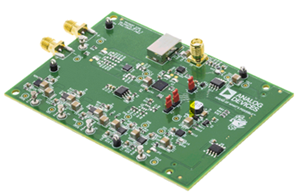
EV1HMC832ALP6G
Analog Devices Inc.The HMC832A is a 3.3 V, high performance, wideband, fractional-N, phase-locked loop (PLL) that features an integrated voltage controlled oscillator (VCO) with a fundamental frequency of 1500 MHz to 3000 MHz and an integrated VCO output divider (divide by 1, 2, 4, 6, ? 62) that enables the HMC832A to generate continuous frequencies from 25 MHz to 3000 MHz. The integrated phase detector (PD) and ?-? modulator, capable of operating at up to 100 MHz, permit wider loop bandwidths and faster frequency tuning with excellent spectral performance.Industry leading phase noise and spurious performance, across all frequencies, enable the HMC832A to minimize blocker effects, and to improve receiver sensitivity and transmitter spectral purity. A low noise floor (?160 dBc/Hz) eliminates any contribution to modulator/mixer noise floor in transmitter applications.The HMC832A is footprint compatible to the market leading HMC830 PLL with an integrated VCO. It features 3.3 V supply and an innovative programmable performance technology that enables the HMC832A to tailor current consumption and corresponding noise floor performance to individual applications by selecting either a low current consumption mode or a high performance mode for an improved noise floor performance.Additional features of the HMC832A include 12 dB of RF output gain control in 1 dB steps; an output mute function to automatically mute the output during frequency changes when the device is not locked; selectable output return loss; programmable differential or single-ended outputs, with the ability to select either output in single-ended mode; and a ?-? modulator exact frequency mode that enables users to generate output frequencies with 0 Hz frequency error; and a register configurable 3.3 V or 1.8 V serial port interface (SPI).Applications Cellular infrastructure Microwave radios WiMax, WiFi Communications test equipment CATV equipment DDS replacement Military Tunable reference sources for spurious-free performance

EV1HMC8415LP6G
Analog Devices Inc.The HMC8415LP6GE is a gallium nitride (GaN), power amplifier, delivering 40 W (46 dBm) with more than 37.5% power added efficiency (PAE) across a bandwidth of 9 GHz to 10.5 GHz.The HMC8415LP6GE is ideal for pulsed applications, such as wireless weather, marine, and military radar applications.APPLICATIONS Weather radars Marine radars Military radars

EV1HMC8500PM5
Analog Devices Inc.The HMC8500PM5E is a gallium nitride (GaN), broadbandpower amplifier delivering 10 W (40 dBm), typical, with up to 55% power added efficiency (PAE) across an instantaneousbandwidth of 0.01 GHz to 2.8 GHz, at an input power of 30 dBm. The typical gain flatness is 3 dB at small signal levels.The HMC8500PM5E is ideal for pulsed or continuous wave(CW) applications, such as wireless infrastructure, radars,public mobile radios, and general-purpose amplification.The HMC8500PM5E amplifier is externally tuned using lowcost, surface-mount components and is available in a compactLFCSP package.Note that, throughout this data sheet, multifunction pins, such as RFIN/VGG, are referred to either by the entire pin name or by a single function of the pin, for example, RFIN, when only that function is relevantAPPLICATIONS Extended battery operation for public mobile radios Power amplifier stage for wireless infrastructures Test and measurement equipment Commercial and military radars General-purpose transmitter amplification

EV1HMC881ALP5
Analog Devices Inc.The HMC881A is a monolithic microwave integrated circuit (MMIC) low-pass filter that features a user-selectable cutoff frequency. The cutoff frequency can be varied from 2.4 GHz to 4 GHz by applying a single analog tuning voltage between 0 V and 14 V. This low-pass filter provides a low 3 dB insertion loss, 16.5 dB return loss, and 1.35 ? f3dB stopband attenuation of >20 dB. This tunable filter can be used as a much smaller alternative to physically large switched filter banks and cavity tuned filters. The HMC881A has excellent microphonics due to the monolithic design, and provides a dynamically adjustable solution in advanced communications applications. The low-pass tunable filter is packaged in a RoHS compliant 5 mm ? 5 mm LFCSP package.Applications Testing and measurement equipment Military radar and electronic warfare/electronic countermeasures (ECMs) Satellite communication and space Industrial and medical equipment

EV1HMC892ALP5
Analog Devices Inc.The HMC892ALP5E is a tunable band-pass filter that features auser selectable pass-band frequency. The 3 dB filter bandwidth isapproximately 8.7%. The 20 dB filter bandwidth is approximately23.8%. The center frequency can be varied between 3.45 GHzand 6.25 GHz by applying an analog tuning voltage between 0 Vand 14 V.This tunable filter can be used as a smaller alternative tophysically large switched filter banks and cavity tuned filters.The HMC892ALP5E has excellent microphonics due to themonolithic design and provides a dynamically adjustablesolution in advanced communications applications. Applications Test and measurement equipment Military radar and electronic warfare (EW)/electronic countermeasures (ECM) Satellite communications (SATCOM) and space Industrial and medical equipment

EV1HMC908ALC5
Analog Devices Inc.The HMC908A is a compact, gallium arsenide (GaAs), monolithic microwave integrated circuit (MMIC), inphase/quadrature (I/Q) downconverter in a leadless, RoHS compliant ceramic leadless chip carrier. This device provides a small signal conversion gain of 11 dB with a noise figure of 2 dB and 25 dB of image rejection at 100 MHz. The HMC908A utilizes a low noise amplifier (LNA) followed by an image rejection mixer that is driven by a local oscillator (LO) buffer amplifier. The image rejection mixer eliminates the need for a filter following the LNA, and removes thermal noise at the image frequency. I and Q mixer outputs are provided and an external 90? hybrid is needed to select the required sideband. The HMC908A is a much smaller alternative to hybrid style image rejection mixer downconverter assemblies, and it eliminates the need for wire bonding by allowing the use of surface-mount manufacturing techniques.Applications Point to point radios Point to multipoint radios and very small aperture terminals (VSATs) Test equipment and sensors Military end use

EV1HMC951ALP4
Analog Devices Inc.The HMC951A is a compact gallium arsenide (GaAs), monolithic microwave integrated circuit (MMIC), in-phase quadrature (I/Q) downconverter in a RoHS compliant package that operates from 5.6 GHz to 8.6 GHz. This device provides a small signal conversion gain of 13 dB with a noise figure of 2 dB and an image rejection of 32 dBc. The HMC951A uses a low noise amplifier (LNA) followed by an image mixer that is driven by a local oscillator (LO) buffer amplifier. The image reject mixer eliminates the need for a filter following the LNA and removes thermal noise at the image frequency. The IF1 and IF2 mixer outputs are provided and an external 90? hybrid is needed to select the required sideband. The I/Q mixer topology reduces the need for filtering of unwanted sideband. The HMC951A is a smaller alternative to hybrid style, single sideband (SSB) downconverter assemblies, and it eliminates the need for wire bonding by allowing the use of surface-mount manufacturing techniques.The HMC951A is available in 4 mm ? 4 mm, 24-lead lead frame chip scale package (LFCSP) and operates over the ?40?C to +85?C temperature range. An evaluation board for the HMC951A is also available upon request. Applications Point to point and point to multipoint radios Military radars, electronic warfare, and electronic intelligence Satellite communications Sensors

EV1HMC973ALP3
Analog Devices Inc.The HMC973ALP3E is an absorptive Voltage VariableAttenuator (VVA) which operates from 0.5 to 5 GHzand is ideal in designs where an analog DC controlsignal must be used to control RF signal levels overa 26 dB amplitude range. It features a shunt-typeattenuator controlled by an analog voltage, Vctrl.The HMC973ALP3E is an unidirectional device withoptimum linearity performance achieved when the RFinput signal is applied to the RFIN package lead. TheHMC973ALP3E is housed in a RoHS compliant 3x3mm QFN leadless package.Applications Point-to-point radio Cellular/3G & WiMAX/4G infrastructure Test instrumentation Microwave sensors? Military, ECM & radar

System-on-Module (SOM) Board to Evaluate the 1 GHz ADSP-2156x SHARC+® Family of Audio Processors
Analog Devices Inc.The EV-21569-SOM with low-cost evaluation and rapid prototyping of the ADSP-2156× Family (ADSP-21562/21563/21565/21566/21567/21569) of SHARC+ audio processors. It features the processor, memory, and power portions of the design and provides an easy-to-use plug-n-play reference design with all the key interfaces made available on three connectors for marrying to either the EV-SOMCRR-EZKIT carrier board or a custom carrier board. The EV-21569-SOM and EV-SOMCRR-EZKIT boards may be purchased as a bundle (EV-21569-EZKIT), providing fast and easy evaluation of the processor core and system peripherals/interfaces.
The EV-21569-SOM module requires the CrossCore® Embedded Studio (CCES) development tools to enable developers to achieve faster time to market. The development environment aids advanced application code development and debug, such as:
Create, compile, assemble, and link application programs written in C++, C, and assembly
Load, run, step, halt, and set breakpoints in application programs
Read and write data and program memory
Read and write core and peripheral registers
When used without the EV-SOMCRR-EZKIT carrier board, the EV-21569-SOM board requires an external in-circuit emulator (ICE-1000 or ICE-2000) be connected to the JTAG header.

System-on-Module (SOM) Board to Evaluate the 1 GHz ADSP-2159x SHARC+® Family of Audio Processors
Analog Devices Inc.The EV-21593-SOM enables evaluation and rapid prototyping of designs featuring the ADSP-2159x Family (ADSP-21591/ADSP-21593) of SHARC audio processors. It provides an easy-to-use plug-n-play reference design with expansion capabilities to interface to custom hardware ahead of the release of the processor itself. When the EV-21593-SOM board is plugged into the EV-SOMCRR-EZKIT carrier board, the resulting EZ-KIT® evaluation system (EV-21593-EZKIT) can be used for fast and easy evaluation of the processor core and system peripherals/interfaces.
The EV-21593-SOM enables rapid prototyping for a wide range of applications, including immersive 3D sound and personal audio zones (PAZ), automotive active and road noise cancellation (ANC/RNC), voice-based user-interfaces and in-car communications (ICC), engine sound synthesis (ESS) and electric vehicle warning sound systems (EVWSS/AVAS). Additional applications include professional audio and soundbars / home AVRs (with 3D Object and Multi-Channel Audio) and enhanced conferencing systems. ADI offers several software modules (e.g., AEC/NR, microphone beamforming, pitch shifting, harmonic generators, wave players etc.), as well as complete software solutions that can be licensed, where users can develop/evaluate their audio and voice processing applications. ADI also offers 3rd party surround sound solutions that can be licensed on ADI’s SHARC processor families. Please visit ADI’s Software Solutions page for more information.
The EV-21593-SOM module utilizes the CrossCore® Embedded Studio (CCES) development tools to enable developers to achieve faster time to market. The development environment aids advanced application code development and debug, such as:
Create, compile, assemble, and link application programs written in C++, C, and assembly
Load, run, step, halt, and set breakpoints in application programs
Read and write data and program memory
Read and write core and peripheral registers

EV2HMC1119LP4M
Analog Devices Inc.The HMC1119 is a broadband, highly accurate, 7-bit digitalattenuator, operating from 0.1 GHz to 6.0 GHz with 31.5 dBattenuation control range in 0.25 dB steps.The HMC1119 is implemented in a silicon process, offeringvery fast settling time, low power consumption, and high ESDrobustness. The device features safe state transitions and isoptimized for excellent step accuracy and high linearity overfrequency and temperature range. The RF input and output areinternally matched to 50 ? and do not require any externalmatching components. The design is bidirectional; therefore,the RF input and output are interchangeable.The HMC1119 has an on-chip regulator that can support a widesupply operating range from 3.3 V to 5.0 V with no performancechange in electrical characteristics. The HMC1119 incorporates adriver that supports serial (3-wire) and parallel controls of theattenuator.The HMC1119 comes in a RoHS-compliant, compact, 4 mm ?4 mm LFCSP package.A fully populated evaluation board is available.Applications Cellular infrastructure Microwave radios and very small aperture terminals (VSATs) Test equipment and sensors IF and RF designs

ADE9153A Arduino Shield Evaluation Board
Analog Devices Inc.The EV-ADE9153ASHIELDZ is an Arduino shield compatible with Arduino Uno, Arduino Zero, or ESP8266. The shield has an on-board shunt resistor for line current measurement and enables quick evaluation and prototyping of energy measurement systems that use the ADE9153A. Arduino library and application examples are provided on the ADE9153A product page to simplify implementation of larger systems. Using mSure® autocalibration, the shield can be calibrated to measure energy with 1% accuracy over the dynamic range without the need for expensive calibration equipment.

EV-ADF4002SD1Z
Analog Devices Inc.The ADF4002 frequency synthesizer is used to implement local oscillators in the up-conversion and down-conversion sections of wireless receivers and transmitters. It consists of a low-noise digital phase frequency detector (PFD), a precision charge pump, a programmable reference divider and programmable N divider. The 14-bit reference counter (R counter), allows selectable REFIN frequencies at the PFD input.A complete phase-locked loop (PLL) can be implemented if the synthesizer is used with an external loop filter and voltage controlled oscillator (VCO). In addition, by programming R and N to 1, the device can be used as a standalone PFD and charge pump.The ADF4002-EP supports defense and aerospace applications (AQEC standard).

EV-ADF4153ASD1Z
Analog Devices Inc.The ADF4153A is a fractional-N frequency synthesizer that implements local oscillators in the upconversion and downconversion sections of wireless receivers and transmitters. It consists of a low noise digital phase frequency detector (PFD), a precision charge pump, and a programmable reference divider. A sigma-delta (?-?) based fractional interpolator allows programmable fractional-N division. The INT, FRAC, and MOD registers define an overall N divider (N = (INT + (FRAC/MOD))). In addition, the 4-bit reference counter (R counter) allows selectable REFIN frequencies at the PFD input. A complete phase-locked loop (PLL) can be implemented if the synthesizer is used with an external loop filter and a voltage controlled oscillator (VCO).A simple 3-wire interface controls all on-chip registers. The device operates with a power supply ranging from 2.7 V to 3.3 V and can be powered down when not in use.Applications CATV equipment Base stations for mobile radio (GSM, PCS, DCS, WiMAX, SuperCell 3G, CDMA, W-CDMA) Wireless handsets (GSM, PCS, DCS, CDMA, W-CDMA) Wireless LANs, PMR Communications test equipment

EV-ADF4196SD1Z
Analog Devices Inc.The ADF4196 frequency synthesizer can be used to implement local oscillators (LO) in the upconversion and downconversion sections of wireless receivers and transmitters. Its architecture isspecifically designed to meet the GSM/EDGE lock time requirements for base stations, and the fast settling feature makes theADF4196 suitable for pulse Doppler radar applications.The ADF4196 consists of a low noise, digital phase frequency detector (PFD) and a precision differential charge pump. A differential amplifier converts the differential charge pump output to a single-ended voltage for the external voltage controlled oscillator (VCO). The sigma-delta (?-?) based fractional interpolator, working with the N divider, allows programmable modulus fractional-N division. Additionally, the 4-bit reference (R) counter and on-chip frequency doubler allow selectable reference signal (REFIN) frequencies at the PFD input.A complete phase-locked loop (PLL) can be implemented if the synthesizer is used with an external loop filter and a VCO. The switching architecture ensures that the PLL settles within the GSM time slot guard period, removing the need for a second PLL and associated isolation switches. This decreases the cost, complexity, PCB area, shielding, and characterization found on previous ping-pong GSM PLL architectures.Applications GSM/EDGE base stations PHS base stations Pulsed Doppler radar Instrumentation and test equipment Beam-forming/phased array systems

EV-ADF4355SD1Z
Analog Devices Inc.The ADF4355 allows implementation of fractional-N or integer-N phase-locked loop (PLL) frequency synthesizers when used with an external loop filter and an external reference frequency. A series of frequency dividers permits operation from 54 MHz to 6800 MHz.The ADF4355 has an integrated VCO with a fundamental output frequency ranging from 3400 MHz to 6800 MHz. In addition, the VCO frequency is connected to divide by 1, 2, 4, 8, 16, 32, or 64 circuits that allow the user to generate radio frequency (RF) output frequencies as low as 54 MHz. For applications that require isolation, the RF output stage can be muted. The mute function is both pin and software controllable.Control of all on-chip registers is through a simple 3-wire interface. The ADF4355 operates with analog and digital power supplies ranging from 3.15 V to 3.45 V, with charge pump and VCO supplies from 4.75 V to 5.25 V. The ADF4355 also contains hardware and software power-down modes.Applications Wireless infrastructure (W-CDMA, TD-SCDMA, WiMAX, GSM, PCS, DCS, DECT) Point to point/point to multipoint microwave links Satellites/VSATs Test equipment/instrumentation Clock generation

EV-ADF4360-3EB1Z
Analog Devices Inc.The ADF4360-3 is a fully integrated integer-N synthesizer andvoltage controlled oscillator (VCO). The ADF4360-3 is designedfor a center frequency of 1750 MHz. In addition, there is adivide-by-2 option available, whereby the user gets an RF output of between 800 MHz and 975 MHz. Control of all the on-chip registers is through a simple 3-wire interface. The device operates with a power supply ranging from 3.0 V to 3.6 V and can be powered down when not in use.?

EV-ADF4360-8EB1Z
Analog Devices Inc.The ADF4360-8 is an integrated integer-N synthesizer and voltagecontrolled oscillator (VCO). The ADF4360-8 center frequencyis set by external inductors. This allows a frequencyrange of between 65 MHz to 400 MHz. Control of all the on-chip registers is through a simple 3-wire interface. The device operates with a power supply ranging from 3.0 V to 3.6 V and can be powered down when not in use.?

EV-ADF4371SD2Z
Analog Devices Inc.The ADF4371 allows implementation of fractional-N or Integer N phase-locked loop (PLL) frequency synthesizers when used with an external loop filter and an external reference frequency. The wideband microwave voltage controlled oscillator (VCO) design allows frequencies from 62.5 MHz to 32 GHz to be generated.The ADF4371 has an integrated VCO with a fundamental output frequency ranging from 4000 MHz to 8000 MHz. In addition, the VCO frequency is connected to divide by 1, 2, 4, 8, 16, 32, or 64 circuits that allows the user to generate radio frequency (RF) output frequencies as low as 62.5 MHz at RF8x. A frequency multiplier at RF16x generates from 8 GHz to 16 GHz. A frequency quadrupler generates frequencies from 16 GHz to 32 GHz at RF32x. RFAUX8x duplicates the frequency range of RF8x or permits direct access to the VCO output. To suppress the unwanted products of frequency multiplication, a harmonic filter exists between the multipliers and the output stages of RF16x and RF32x.Control of all on-chip registers is through a 3-wire interface. The ADF4371 operates with analog and digital power suppliesranging from 3.15 V to 3.45 V, and 5 V for the VCO power supply. The ADF4371 also contains hardware and software power-down modes. APPLICATIONS Wireless infrastructure (multicarrier global system for mobile communication (MC-GSM), 5 G) Test equipment and instrumentation Clock generation Aerospace and defense

EV-ADF5610SD1Z
Analog Devices Inc.The ADF5610 allows implementation of fractional-N or Integer N phase-locked loop (PLL) frequency synthesizers when used with an external loop filter and an external reference source. The wideband microwave voltage controlled oscillator (VCO) design permits frequency operation from 7300 MHz to 14600 MHz at a single radio frequency (RF) output. A series of frequency dividers with a differential frequency output allows operation from 57 MHz to 14600 MHz. Analog and digital power supplies for the PLL circuitry range from 3.1 V to 3.5 V, and the VCO supplies are between 4.75 V and 5.25 V. The charge pump supply voltage can be extended up to 3.6 V for improved frequency band overlap and extended upper frequency range.The ADF5610 has an integrated VCO with a fundamental frequency of 3650 MHz to 7300 MHz. These frequencies are internally doubled and routed to the RFOUT pin. An additional differential output allows the doubled VCO frequency to be divided by 1, 2, 4, 8, 16, 32, 64, or 128, allowing the user to generate RF output frequencies as low as 57 MHz. A simple 3?wire serial port interface (SPI) provides control of all on-chip registers. To conserve power, this divider block can be disabled when not needed through the SPI interface. Likewise, the output power for both the single-ended output and the differential output are programmable via the VCO register settings. The ADF5610 also contains various power-down modes for the VCO circuitry and PLL circuitry.The integrated phase detector (PD) and delta-sigma (?-?) modulator, capable of operating at up to 100 MHz, permit wide loop bandwidths and fast frequency tuning with a typical spurious level of ?100 dBc.With phase noise levels from ?115 dBc/Hz at 7.3 GHz to ?109 dBc/Hz at 14.6 GHz, the ADF5610 is equipped to minimize blocker effects, and to improve receiver sensitivity and transmitter spectral purity. The low phase noise floor eliminates any contribution to modulator and mixer noise floor in transmitter applications.The ADF5610 is a PLL with integrated VCO. The device features an innovative programmable performance technology that enables the ADF5610 to tailor current consumption and corresponding noise performance to individual applications by selecting either a low current consumption mode or a high performance mode for improved phase noise performance.Additional features of the ADF5610 include approximately 3 dBof RFOUT gain control in 1.5 dB steps and 5 dB of control onthe differential port in approximately 2.5 dB steps. Finally, the ?-?modulator with exact frequency mode enables users to generateoutput frequencies with 0 Hz frequency error.APPLICATIONSMilitary and defenseTest equipmentClock generationWireless infrastructureSatellite and very small aperture terminal (VSAT)Microwave radio