Top Manufacturers
Stock

Displaying 1041 - 1060 of 5453

Evaluation Kits from Analog Devices Inc.

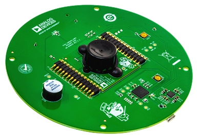
The ADuCM4050WL EZ-KIT® from Analog Devices, Inc. is an evaluation system for the ADuCM4050 processor

Analog Devices Inc.
The ADuCM4050WL EZ-KIT® and ADuCM4050LF EZ-KIT®, Analog Devices, Inc. are an evaluation system for the ADuCM4050 MCU, for the WLCSP and LFCSP packages respectively. The ADuCM4050 processor is an ultra low-power integrated mixed-signal microcontroller system for processing, control and connectivity. The MCU system is based on the ARM Cortex-M4F processor. The MCU also has a collection of digital peripherals, embedded SRAM and flash memory, and an analog subsystem which provides clocking, reset, and power management capability in addition to an ADC subsystem. The EZ-KIT contains an array of three connectors that support the ADF7xxx Wireless Transceiver series of daughterboard products. Refer to ADF7xxx Wireless Transceiver Daughterboard Interface for more information. The EZ-KIT contains Expansion Interface 3 (EI3) and Arduino interfaces. These interfaces provide connections for daughterboards to expand the functionality of the EZ-KIT. Refer to Expansion Interface 3 and Arduino Interface for more information. The evaluation board is designed to be used with with the IAR, Keil or CrossCore Embedded Studio development environments for advanced application code development and debug, such as: Create, compile, assemble, and link application programs written in C++, C, and assembly Load, run, step, halt, and set breakpoints in application programs Read and write data and program memory Read and write core and peripheral registers

EVAL-ADCMP607BCPZ

Analog Devices Inc.
The ADCMP606 and ADCMP607 are very fast comparatorsfabricated on XFCB2, an Analog Devices, Inc., proprietaryprocess. These comparators are exceptionally versatile and easyto use. Features include an input range from VEE ? 0.5 V toVCCI + 0.2 V, low noise, CML-compatible output drivers, andTTL-/CMOS-compatible latch inputs with adjustable hysteresisand/or shutdown inputs.The devices offer 1.25 ns propagation delay with 2.5 ps rmsrandom jitter (RJ). Overdrive and slew rate dispersion aretypically less than 50 ps.A flexible power supply scheme allows the devices to operatewith a single +2.5 V positive supply and a ?0.5 V to +2.7 Vinput signal range up to a +5.5 V positive supply with a ?0.5 Vto +5.7 V input signal range. The ADCMP607 features splitinput/output supplies with no sequencing restrictions tosupport a wide input signal range with independent outputswing control and power savings.The CML-compatible output stage is fully back-matched forsuperior performance. The comparator input stage offers robustprotection against large input overdrive, and the outputs do notphase reverse when the valid input signal range is exceeded. Onthe ADCMP607, latch and programmable hysteresis features arealso provided with a unique single-pin control option.The ADCMP606 is available in a 6-lead SC70 package and theADCMP607 is available in a 12-lead LFCSP package.Applications High speed instrumentation Clock and data signal restoration Logic level shifting or translation Pulse spectroscopy High speed line receivers Threshold detection Peak and zero-crossing detectors High speed trigger circuitry Pulse-width modulators Current-/voltage-controlled oscillators Automatic test equipment (ATE)

EVAL-ADV7802EB1Z

Analog Devices Inc.
Video IC Development Tools EVAL BRD ADV7802

EVAL-AD7705EBZ

Analog Devices Inc.
The AD7705 / AD7706?are complete analog front ends for low frequency measurement applications. These 2-/3-channel devices can accept low level input signals directly from a transducer and produce serial digital output. The devices employ a ?-? conversion technique to realize up to 16 bits of no missing codes performance. The selected input signal is applied to a proprietary, programmable-gain front end based around an analog modulator. The modulator output is processed by an on-chip digital filter. The first notch of this digital filter can be programmed via an on-chip control register, allowing adjustment of the filter cutoff and output update rate. The AD7705 / AD7706 devices operate from a single 2.7 V to 3.3 V or 4.75 V to 5.25 V supply. The AD7705 features two fully differential analog input channels; the AD7706 features three pseudo differential input channels. Both devices feature a differential reference input. Input signal ranges of 0 mV to 20 mV through 0 V to 2.5 V can be incorporated on both devices when operating with a VDD of 5 V and a reference of 2.5 V. They can also handle bipolar input signal ranges of ?20 mV through ?2.5 V, which are referenced to the AIN(?) inputs on the AD7705 and to the COMMON input on the AD7706.The AD7705 / AD7706 devices, with a 3 V supply and a 1.225 V reference, can handle unipolar input signal ranges of 0 mV to 10 mV through 0 V to 1.225 V. The devices can accept bipolar input ranges of ?10 mV through ?1.225 V. Therefore, the AD7705 / AD7706 devices perform all signal conditioning and conversion for a 2-channel or 3-channel system. The AD7705 / AD7706 are ideal for use in smart, microcontroller, or DSP-based systems. The devices feature a serial interface that can be configured for 3-wire operation. Gain settings, signal polarity, and update rate selection can be configured in software using the input serial port. The parts contains self-calibration and system calibration options to eliminate gain and offset errors on the part itself or in the system. CMOS construction ensures very low power dissipation, and the power-down mode reduces the standby power consumption to 20 ?W typ. These parts are available in a 16-lead, wide body (0.3 inch), plastic dual in-line package (DIP); a 16-lead, wide body (0.3 inch), standard small outline (SOIC) package; and a low profile, 16-lead, thin shrink small outline package (TSSOP).

EVAL-ADG901EBZ

Analog Devices Inc.
The ADG901/ADG902 are wideband switches that use a complementary metal-oxide semiconductor (CMOS) process to provide high isolation and low insertion loss to 1 GHz. The ADG901 is an absorptive (matched) switch with 50 ? terminated shunt legs, while the ADG902 is a reflective switch. These devices are designed such that the isolation is high over the dc to 1 GHz frequency range. These switches enable the user to pass dc signals up to 0.5 V without the use of a dc blocking capacitor. They have on-board CMOS control logic, thus eliminating the need for external controlling circuitry. The control inputs are both CMOS and LVTTL compatible. The low power consumption of these CMOS devices makes them ideally suited to wireless applications and general-purpose high frequency switching.Product Highlights 40 dB Off Isolation at 1 GHz 0.8 dB Insertion Loss at 1 GHz 17 dBm P1dB at 1 GHzApplications Wireless communications General purpose RF switching Dual-band applications High speed filter selection Digital transceiver front-end switch IF switching Tuner modules Antenna diversity switching list

LTM4636-1PolyPhase 160A Step-Down Power µModule Regulator with Overvoltage and Overtemperature Protection

Analog Devices Inc.
Demonstration circuit DC2448A-D features a PolyPhase® design using the LTM4636-1EY, a 40A high efficiency, switch mode step-down power µModule® regulator with overvoltage and overtemperature protection features. The input voltage range is from 9V to 15V. The output voltage range is 0.6V to 3.3V. The DC2448A-D can deliver a nominal 160A output current. DC2448A-D has on-boardhot swap circuit that can disconnect input supply and protect the LTM4636-1 and the load under overvoltage and overtemperature conditions. As explained in the data sheet, output current derating is necessary for certain VIN, VOUT and thermal conditions. The board operates in continuous conduction mode in heavy load conditions. For high efficiency at low load currents, the MODE_PLLIN jumper selects pulse-skipping mode for noise sensitive applications or Burst Mode® operation in less noise sensitive applications. The MODE_PLLIN pin also allows the LTM4636-1 to synchronize to an external clock signal. DC2448A-D has the option of choosing both internal and external compensation circuits for LTM4636-1. The LTM4636-1 data sheet must be read in conjunction with this demo manual prior to working on or modifying demo circuit DC2448A-D.

AD9689-2600EBZ

Analog Devices Inc.
The AD9689 is a dual, 14-bit, 2.0 GSPS/2.6 GSPS analog-to-digital converter (ADC). The device has an on-chip buffer and a sample-and-hold circuit designed for low power, small size, and ease of use. This product is designed to support communications applications capable of direct sampling wide bandwidth analog signals of up to 5 GHz. The ?3 dB bandwidth of the ADC input is 9 GHz. The AD9689 is optimized for wide input bandwidth, high sampling rate, excellent linearity, and low power in a small package.The dual ADC cores feature a multistage, differential pipelined architecture with integrated output error correction logic. Each ADC features wide bandwidth inputs supporting a variety of user-selectable input ranges. An integrated voltage reference eases design considerations. The analog input and clock signals are differential inputs. The ADC data outputs are internally connected to four digital downconverters (DDCs) through a crossbar mux. Each DDC consists of multiple cascaded signal processing stages: a 48-bit frequency translator (numerically controlled oscillator (NCO)), and decimation rates. The NCO has the option to select preset bands over the general-purpose input/output (GPIO) pins, which enables the selection of up to three bands. Operation of the AD9689 between the DDC modes is selectable via SPI-programmable profiles.In addition to the DDC blocks, the AD9689 has several functions that simplify the automatic gain control (AGC) function in a communications receiver. The programmable threshold detector allows monitoring of the incoming signal power using the fast detect control bits in Register 0x0245 of the ADC. If the input signal level exceeds the programmable threshold, the fast detect indicator goes high. Because this threshold indicator has low latency, the user can quickly turn down the system gain to avoid an overrange condition at the ADC input. In addition to the fast detect outputs, the AD9689 also offers signal monitoring capability. The signal monitoring block provides additional information about the signal being digitized by the ADC.The user can configure the Subclasss 1 JESD204B-based high speed serialized output in a variety of one-lane, two-lane, four-lane, and eight-lane configurations, depending on the DDC configuration and the acceptable lane rate of the receiving logic device. Multidevice synchronization is supported through the SYSREF? and SYNCINB? input pins.The AD9689 has flexible power-down options that allow significant power savings when desired. All of these features can be programmed using a 3-wire serial port interface (SPI).The AD9689 is available in a Pb-free, 196-ball BGA, specified over the ?40?C to +85?C ambient temperature range. This product is protected by a U.S. patent.Note that throughout this data sheet, multifunction pins, such as FD_A/GPIO_A0, are referred to either by the entire pin name or by a single function of the pin, for example, FD_A, when only that function is relevant.Product Highlights Wide, input ?3 dB bandwidth of 9 GHz supports direct radio frequency (RF) sampling of signals up to about 5 GHz. Four integrated, wideband decimation filters and NCO blocks supporting multiband receivers. Fast NCO switching enabled through the GPIO pins. SPI controls various product features and functions to meet specific system requirements. Programmable fast overrange detection and signal monitoring. On-chip temperature diode for system thermal management. 12 mm ? 12 mm, 196-ball BGA. Pin, package, feature, and memory map compatible with the AD9208 14-bit, 3.0 GSPS, JESD204B dual ADC.Applications Diversity multiband and multimode digital receivers 3G/4G, TD-SCDMA, W-CDMA, and GSM, LTE, LTE-A Electronic test and measurement systems Phased array radar and electronic warfare DOCSIS 3.0 CMTS upstream receive paths HFC digital reverse path receivers

EVAL01-HMC1060LP3E

Analog Devices Inc.
The HMC1060LP3E is a BiCMOS ultra low noise quad-output linear voltage regulator targeted at high performance applications requiring superb power supply isolation.Maximum 500 mA of current, distributed between four independent outputs, enable the HMC1060LP3E to supply all of the power needs of Hittite's Wideband PLL with Integrated VCO products, such as the HMC830LP6GE.Although targeted at Hittite's Wideband PLLs with Integrated VCO products, the HMC1060LP3E makes an excellent general purpose regulator that supports adjustable output voltages ranging anywhere from 1.8V to 5.2V.An Integrated PTAT (Proportional To Absolute Temperature) feature enabled via an external pin, allows the HMC1060LP3E to scale the supply voltage with temperature in order to maximize phase noise and output power performance of Hittite's Wideband with Integrated VCO products, as well as other devices powered by the HMC1060LP3E.Integrated thermal protection disables the outputs of the HMC1060LP3E at extreme temperatures, until the device cools down, making the HMC1060LP3E a robust device capable of dealing with temporary and unforeseen scenarios including momentary short circuits and extreme temperatures.External Enable input provides a convenient way to power on or off all of the devices supplied by the HMC1060LP3E.The HMC1060LP3E is housed in a 3 ? 3 mm QFN SMT package.APPLICATIONS Ultra Low Noise Frequency Generation?(PLLs, VCOs, PLLs?with Integrated VCOs) RF & Mixed-Signal Supply

EVAL-AD7732EBZ

Analog Devices Inc.
The AD7732 is a high precision, high throughput analog front end. True 16-bit peak-to-peak resolution is achievable with total conversion times of 500 ?s (2 kHz channel switching) making it ideally suitable for high resolution multiplexing applications.The part can be configured via a simple digital interface, which allows users to balance the noise performance against data throughput up to a 15.4 kHz.The analog front end features two fully differential input channels with unipolar or true bipolar input ranges to ?10 V while operating from a single +5 V analog supply. The part has an overrange and underrange detection capability and accepts an analog input overvoltage to ?16.5 V without degrading the performance of the adjacent channels.The differential reference input features ?No-Reference? detect capability. The ADC also supports per channel system calibration options. The digital serial interface can be configured for 3-wire operation and is compatible with microcontrollers and digital signal processors. All interface inputs are Schmitt triggered. The part is specified for operation over the extended industrial temperature range of ?40?C to +105?C and is available in 28-lead TSSOP package.Other parts in the AD7732 family are the AD7734?and the AD7738.The AD7734 is similar to AD7732, but its analog front end features four single-ended input channels.The AD7738 analog front end is configurable for four fully differential or eight single-ended input channels, features 0.625 V to 2.5 V bipolar/unipolar input ranges, and accepts a common-mode input voltage from 200 mV to AVDD ? 300 mV. The AD7738 multiplexer output is pinned out externally, allowing the user to implement programmable gain or signal conditioning before being applied to the ADC.APPLICATIONS PLCs/DCS Multiplexing applications Process control Industrial instrumentation

ADCA5191-EVALZ

Analog Devices Inc.
The ADCA5191 is a medium power gain block amplifier that provides excellent linearity across a flexible bias range allowing power efficient design implementation for various applications.The device provides 25.8 dB of flat gain up to 1800 MHz, making this ideal for Data Over Cable Service Interface Specification (DOCSIS) 4.0 downstream applications. The device is also well suited for upstream applications to 700 MHz as the output stage. It is conveniently packaged in an industry-standard, 5 mm ? 5 mm, 32-lead, lead frame chip-scale package (LFCSP) with an exposed pad on the bottom of the package for improved thermal performance.APPLICATIONS45 MHz to 1800 MHz CATV infrastructure amplifier systems5 MHz to 700 MHz upstreamRemote physical layer (PHY)DOCSIS? 3.1 and DOCSIS 4.0 compliant

LTC7800 Demo Board | 8 ≥ VIN ≥ 40V, VOUT = 3.3V @ 10A

Analog Devices Inc.
Demonstration circuit 2786A is a single output high voltage non-isolated synchronous step-down converter that drives an all N-channel MOSFET power stage. It features the LTC7800, a low quiescent current high frequency (programmable fixed frequency from 320kHz up to 2.25MHz) synchronous step-down DC/DC controller housed in a small 3mm x 4mm QFN package. This DC2786A operates over an input voltage range from 8V to 40V, while the LTC7800 can operate up to 60V. This demo board produces a 3.3V output voltage with up to 10A output current, and is configured with a sense resistor for current sensing. A mode selector allows the DC2786A to operate in forced continuous operation, pulse-skipping or Burst Mode® operation during light loads. The LTC7800 features two integrated 5V gate drivers with 20ns deadtime which is good for GaN transistors or logic-level MOSFETs to maximize efficiency. The EXTVCC pin permits the LTC7800 to be powered from the output of the switching regulator or other available source, reducing power dissipation and improving efficiency. Please refer to the LTC7800 data sheet for a complete description of the part operation and application information.

EVAL-ADM2487EEB5Z

Analog Devices Inc.
The ADM2482E/ADM2487E are isolated data transceivers with ?15 kV ESD protection and are suitable for high speed, half-duplex or full-duplex communication on multipoint transmission lines. For half-duplex operation, the transmitter outputs and receiver inputs share the same transmission line. Transmitter Output Pin Y is linked externally to Receiver Input Pin A, and Transmitter Output Pin Z to Receiver Input Pin B. The parts are designed for balanced transmission lines and comply with TIA/EIA- 485-A-98 and ISO 8482:1987(E).The devices employ the Analog Devices, Inc., iCoupler? technology to combine a 3-channel isolator, a three-state differential line driver, and a differential input receiver into a single package. An on-chip oscillator outputs a pair of square waveforms that drive an external transformer to provide isolated power. The logic side of the device can be powered with either a 5 V or a 3.3 V supply, and the bus side is powered with an isolated 3.3 V supply.The ADM2482E/ADM2487E driver has an active high enable, and the receiver has an active low enable. The driver output enters a high impedance state when the driver enable signal is low. The receiver output enters a high impedance state when the receiver enable signal is high.The device has current-limiting and thermal shutdown features to protect against output short circuits and situations where bus contention might cause excessive power dissipation. The part is fully specified over the industrial temperature range of ?40?C to +85?C and is available in a 16-lead, wide-body SOIC package.Applications Isolated RS-485/RS-422 interfaces Industrial field networks Multipoint data transmission systems

EVAL-ADM1063TQEBZ

Analog Devices Inc.
The ADM1063 is a configurable supervisory/sequencing device that offers a single-chip solution for supply monitoring and sequencing in multiple supply systems. In addition to these functions, the ADM1063 integrates a 12-bit ADC that can be used to accurately read back up to 12 separate voltages.The device also provides up to 10 programmable inputs for monitoring under, over, or out-of-window faults on up to 10 supplies. In addition, 10 programmable outputs can be used as logic enables. Six of these programmable outputs can provide up to a 12 V output for driving the gate of an n-FET that can be placed in the path of a supply.ApplicationsCentral office systems Servers/routers Multivoltage system line cards DSP/FPGA supply sequencing In-circuit testing of margined supplies

LT3472EDD | Boost and Inverting DC/DC Converters, VIN = 2.7V – 4.2V, VOUT1 = 15V @ 25mA–45mA, VOUT2 = –8V @ 35mA–65mA

Analog Devices Inc.
Demonstration circuit 760 is a dual, output, 1.1MHz Boost/Inverter in a 3mm x 3mm DFN featuring the LT3472EDD. The demo circuit demonstrates small size and low component count in a Boost Circuit and an Inverting Circuit. The Boost Converter is designed to convert a 2.7V–4.2V input to 15V output at 25mA– 45mA load. The Inverting Circuit generates a –8V output at 35mA–65mA from the same input. Since the maximum VIN of the LT3472EDD is 16V, this demo circuit will work well at higher inputs. The only limitation is the 10V rating of the input capacitor.

EVAL01-HMC835LP6G

Analog Devices Inc.
The HMC835LP6GE is a low noise, wide band, Fractional-N PLL that features an integrated VCO with a fundamental frequency of 2020 to 4100 MHz, and an integrated VCO Output Divider (divide by 2/4/6/.../60/62) that together enable the HMC835LP6GE to generate frequencies from 33 MHz to 4100 MHz. Integrated Phase Detector (PD) and a deltasigma modulator capable of operating at up to 100 MHz enable wider loop-bandwidths, faster frequency changes along with excellent spectral performance.Two independent RF outputs, with independent gain control, enable the HMC835LP6GE to distribute identical frequency and phase signals to multiple destinations, at optimal signal levels tailored to each output.External VCO input, allows the HMC835LP6GE to lock external VCOs, and enables cascaded LO architectures for MIMO radio applications. Two separate Charge Pump (CP) outputs enable separate loop filters optimized for both integrated and external VCOs, and seamless switching between integrated or external VCOs during operation. Programmable RF output phase feature can further phase adjust and synchronize multiple HMC835LP6GEs enabling scalable MIMO and beam-forming radio architectures.Additional features include configurable output mute function that mutes RF outputs during frequency changes, Exact Frequency Mode that enables the HMC835LP6GE to generate fractional frequencies with 0 Hz frequency error, and the ability to synchronously change frequencies without changing the phase of the output signal.Applications MIMO Radio Architectures Cellular Infrastructure Cellular backhaul Communications Test Equipment CATV Equipment Phased Array Applications? DDS Replacement

LT8316 Demo Board | Isolated Flyback Converter: 100V to 600VIN, VOUT = 12V @ Up to 3A

Analog Devices Inc.
Demonstration circuit 2718A is a no-opto flyback converter featuring the LT8316. The demo board outputs 12V and maintains tight regulation with a load current from 30mA to 3A. It is optimized to operate over a wide 100V to 600V DC input voltage range. Output voltage accuracy stays within ±5% over the entire input voltage and load range. The LT8316 is a high voltage flyback controller. No optoisolator is needed for regulation. The part samples the output voltage from the isolated flyback waveform appearing across a third winding on the transformer. Quasi-resonant boundary mode operation improves load regulation. The LT8316 is available in a thermally enhanced 20-pin TSSOP package with four pins removed for high-voltage spacing. The LT8316 data sheet gives a complete description of the part, operation and application information. The data sheet must be read in conjunction with this quick start guide for demo circuit 2718A.

AD9520-1/PCBZ

Analog Devices Inc.
The AD9520-11 provides a multioutput clock distributionfunction with subpicosecond jitter performance, along with anon-chip PLL and VCO. The on-chip VCO tunes from 2.27 GHzto 2.65 GHz. An external 3.3 V/5 V VCO/VCXO of up to 2.4 GHzcan also be used.The AD9520 serial interface supports both SPI and I2C? ports. An in-package EEPROM can be programmed through the serial interface and store user-defined register settings for power-up and chip reset.The AD9520 features 12 LVPECL outputs in four groups. Anyof the 1.6 GHz LVPECL outputs can be reconfigured as two250 MHz CMOS outputsEach group of outputs has a divider that allows both the divideratio (from 1 to 32) and the phase (coarse delay) to be set.The AD9520 is available in a 64-lead LFCSP and can be operatedfrom a single 3.3 V supply. The external VCO can have anoperating voltage up to 5.5 V. A separate output driver powersupply can be from 2.375 V to 3.465 VThe AD9520 is specified for operation over the standard industrialrange of ?40?C to +85?C.1The AD9520 is used throughout this data sheet to refer to all the members of the AD9520 family. However, when AD9520-1 is used, it is referring to that specificmember of the AD9520 family.ApplicationsLow jitter, low phase noise clock distributionClock generation and translation for SONET, 10Ge, 10G FC, and other 10 Gbps protocolsForward error correction (G.710)Clocking high speed ADCs, DACs, DDSs, DDCs, DUCs, MxFEsHigh performance wireless transceiversATE and high performance instrumentationBroadband infrastructures

DC093A

Analog Devices Inc.
The LT1371 is a monolithic high frequency current mode switching regulator. It can be operated in all standard switching configurations including boost, buck, flyback, forward, inverting and ?Cuk?. A 3A high efficiency switch is included on the die, along with all oscillator, control and protection circuitry.The LT1371 typically consumes only 4mA quiescent current and has higher efficiency than previous parts. High frequency switching allows for very small inductors to be used.New design techniques increase flexibility and maintain ease of use. Switching is easily synchronized to an external logic level source. A logic low on the Shutdown pin reduces supply current to 12?A. Unique error amplifier circuitry can regulate positive or negative output voltage while maintaining simple frequency compensation techniques. Nonlinear error amplifier transconductance reduces output overshoot on start-up or overload recovery. Oscillator frequency shifting protects external components during overload conditions.Applications Boost Regulators Laptop Computer Supplies Multiple Output Flyback Supplies Inverting Supplies

EVAL-ADF7024DB1Z

Analog Devices Inc.
The ADF7024 is an ultralow power, integrated transceiver for use in the license-free ISM bands at 433 MHz, 868 MHz, and 915 MHz. Its ease of use and high performance make it suitable for a wide variety of wireless applications. The ADF7024 is suitable for operation under the European ETSI EN 300-220 regulation, the North American FCC Part 15 regulation, and other similar regulatory standards.The ADF7024 can operate under a number of predefined radio profiles. For each radio profile, optimized register settings are provided for the ADF7024 radio. This ensures that the RF communication layer works seamlessly, allowing the user to concentrate on the protocol and system level design and prototyping. The radio profiles cover common data rate and modulation options. There are six radio profiles in total, as shown in Table 1.The ADF7024 operates with a power supply range of 2.2 V to 3.6 V and has very low power consumption in both Tx and Rx modes, enabling long lifetimes in battery-operated systems while maintaining excellent RF performance.The low IF receiver minimizes power consumption and provides excellent sensitivity. The receiver is exceptionally linear and, therefore, is very resilient to the presence of interferers in spectrally noisy environments. The highly efficient transmitter has programmable output power up to 13.5 dBm and automatic power amplifier (PA) ramping to meet transient spurious specifications. The RF synthesizer comprises a voltage controlled oscillator (VCO), a low noise fractional-N phase-locked loop (PLL) and a loop filter, all of which are fully integrated and automatically calibrated. This agile frequency synthesizer facilitates the implementation of frequency-hopping spread spectrum (FHSS) systems.The smart wake mode (SWM) allows the ADF7024 to wake up autonomously from sleep using the internal wake-up timer without intervention from the host processor. This functionality allows carrier sense, packet sniffing, and packet reception while the host processor is in sleep, thereby reducing overall system current consumption.The ADF7024 eases the processing burden of the host processor by integrating the lower layers of a typical communication protocol stack. The host processor can configure the ADF7024 using a simple command-based protocol over a standard 4-wire SPI interface. A single-byte command transitions the radio between states or performs a radio function.A complete wireless solution can be built using a small number of external discrete components and a host processor (typically a microcontroller).For more information, see the ADF7024 Hardware Reference Manual, UG-698, which is only available as part of the ADF7024 design resource package.APPLICATIONS Wireless sensor networks (WSNs) Home and building automation Asset tracking Process and building control Industrial control Internet of Things (IoT)

DC633A

Analog Devices Inc.
The LTC3202 is a low noise, constant frequency charge pump DC/DC converter that uses fractional conversion to increase efficiency in white LED applications. The part can be used to produce a regulated voltage or current of up to 125mA from a 2.7V to 4.5V input. Low external parts count (two flying capacitors and two small bypass capacitors at VIN and VOUT) make the LTC3202 ideally suited for small, battery-powered applications.An internal 2-bit DAC allows LED current to be adjusted for LED brightness control. The LTC3202 also has thermal shutdown protection and can survive a continuous short-circuit from VOUT to GND. Built-in soft-start circuitry prevents excessive inrush current during start-up. High switching frequency enables the use of small external capacitors. A low current shutdown feature disconnects the load from VIN and reduces quiescent current to less than 1?A.The LTC3202 is available in the 10-pin MSOP and 3mm x 3mm DFN packages.Applications White LED Backlighting Programmable Boost Current Source?

Displaying 1041 - 1060 of 5453

Latest Parts

IN STOCK 13664
Buy

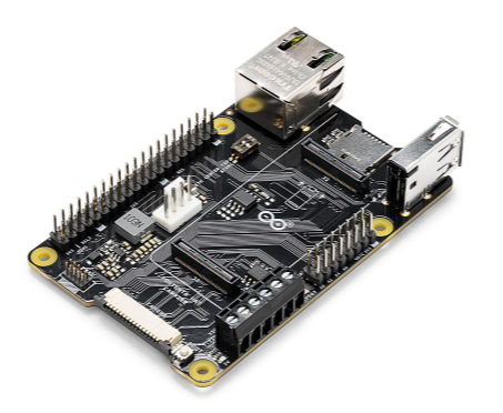
ASX00049

Arduino

* $43.36 - * $50.31

IN STOCK 2847
Buy

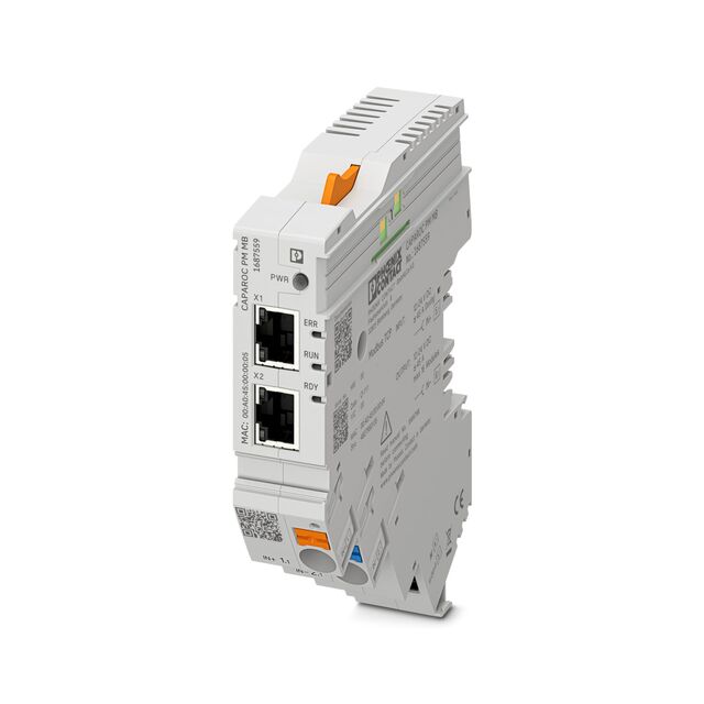
1687559

Phoenix Contact Ltd

[no prices available]

IN STOCK 2
Buy

Reference Designs

RD006

Wurth Elektronik

RD006 - 3 W Dual-output isolated auxiliary supply for communication interfaces and measurement systems

CN0583

Analog Devices Inc.

Multistandard Micropower Verified Smoke Detection System-on-Module

Technical Resources

EVALUATION KITS

EVAL-AD7124-8SDZ

Analog Devices Inc.

$0.00 - * $79.04

IN STOCK 792
Buy
View All