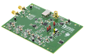
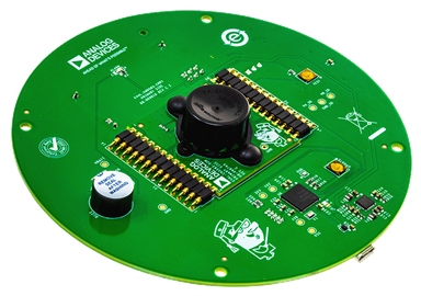
AD737-EVALZ
Analog Devices Inc.The AD737 is a low power, precision, monolithic, true rms-to-dc converter. It is laser trimmed to provide a maximum error of ?0.2 mV ? 0.3% of reading with sine wave inputs. Furthermore, it maintains high accuracy while measuring a wide range of input waveforms, including variable duty cycle pulses and triac (phase) controlled sine waves. The low cost and small physical size of this converter make it suitable for upgrading the performance of non-rms precision rectifiers in many applications. Compared to these circuits, the AD737 offers higher accuracy at equal or lower cost.The AD737 computes the rms value of both the ac and dc input voltages, and is ac-coupled by adding an input capacitor. In this mode, the AD737 can resolve input signal levels of 100 ?V rms or less, despite variations in temperature or supply voltage. High accuracy is maintained for input waveforms with crest factors of 1 to 3 and crest factors at 2.5% or less with respect to full-scale input level.The AD737 has no output buffer amplifier, thereby significantly reducing dc offset errors occurring at the output, which makes the device highly compatible with high input impedance ADCs.Requiring only 160 ?A of power supply current, the AD737 is optimized for use in portable multimeters and other battery-powered applications. In power-down mode, the standby supply current in is typically 25 ?A.The AD737 has both high (1012 ?) and low impedance input options. The high-Z FET input connects high source impedance input attenuators, and a low impedance (8 k?) input accepts rms voltages of up to 0.9 V while operating from the minimum power supply voltage of ?2.5 V. The two inputs can be used either single ended or differentially.The AD737 achieves 1% of reading error bandwidth, exceeding 10 kHz for input amplitudes from 20 mV rms to 200 mV rms, while consuming only 0.72 mW.The AD737 is available in two performance grades. The AD737J and AD737K grades operate over the commercial temperature range of 0?C to 70?C. The AD737JR-5 is tested with supply voltages of ?2.5 V dc. The AD737A grade operates over the industrial temperature range of ?40?C to +85?C. The AD737 is available in two low cost, 8-lead packages: PDIP and SOIC_N.PRODUCT HIGHLIGHTS Computes average rectified, absolute, or true rms value of a signal regardless of waveform. Only one external component, an averaging capacitor, is required for the AD737 to perform true rms measurement. The standby power consumption of 125 ?W makes the AD737 suitable for battery-powered applications.
AD8039ART-EBZ
Analog Devices Inc.The AD8038 (single) and AD8039 (dual) amplifiers are high speed (350 MHz) voltage feedback amplifiers with an exceptionally low quiescent current of 1.0 mA/amplifier typical (1.5 mA maximum). The AD8038 single amplifier in the 8-lead SOIC package has a disable feature. Despite being low power and low cost, the amplifier provides excellent overall performance. Additionally, it offers a high slew rate of 425 V/?s and a low input offset voltage of 3 mV maximum.The Analog Devices, Inc., proprietary XFCB process allows low noise operation (8 nV/?Hz and 600 fA/?Hz) at extremely low quiescent currents. Given a wide supply voltage range (3 V to 12 V), wide bandwidth, and small packaging, the AD8038 and AD8039 amplifiers are designed to work in a variety of applications where power and space are at a premium.The AD8038 and AD8039 amplifiers have a wide input common-mode range of 1 V from either rail and swing to within 1 V of each rail on the output. These amplifiers are optimized for driving capacitive loads up to 15 pF. If driving larger capacitive loads, a small series resistor is needed to avoid excessive peaking or overshoot.The AD8039 amplifier is available in a 8-lead SOT-23 package, and the single AD8038 is available in both an 8-lead SOIC and a 5-lead SC70 package. These amplifiers are rated to work over the industrial temperature range of ?40?C to +85?C.Applications Battery-powered instrumentation Filters A/D drivers Level shifting Buffering Photo multipliers
AD8040AR-EBZ
Analog Devices Inc.The AD8040 is a quad, rail-to-rail input and output high speed amplifier with a quiescent current of only 1.3 mA per amplifier. Despite its low power consumption, the amplifier provides excellent performance with 125MHz small signal bandwidth and 60 V/?s slew rate. ADI's proprietary XFCB process enables high speed and high performance on low power.This amplifier exhibits true single-supply operation with rail-to-rail input and output performance for supply voltages ranging from 2.7V to 12V. The input voltage range extends 200 mV beyond each rail without phase reversal. The dynamic range of the output extends to within 40 mV of each rail.The AD8040 provides excellent signal quality with minimal power dissipation. At G=+1, SFDR is -72dBc at 1MHz and settling time to 0.1% is only 80 ns. Low distortion and fast settling performance makes this amplifier a suitable driver for single-supply A/D converters.The versatility of the AD8040 allows the user to operate the amplifier on a wide range of supplies while consuming less than 6.5 mW of power. This feature extends the operation time in applications ranging from battery-powered systems with large bandwidth requirements to high speed systems where component density requires lower power dissipation.The amplifier is rated over the extended industrial temperature range, -40?C to +125?C.
AD8040ARU-EBZ
Analog Devices Inc.The AD8040 is a quad, rail-to-rail input and output high speed amplifier with a quiescent current of only 1.3 mA per amplifier. Despite its low power consumption, the amplifier provides excellent performance with 125MHz small signal bandwidth and 60 V/?s slew rate. ADI's proprietary XFCB process enables high speed and high performance on low power.This amplifier exhibits true single-supply operation with rail-to-rail input and output performance for supply voltages ranging from 2.7V to 12V. The input voltage range extends 200 mV beyond each rail without phase reversal. The dynamic range of the output extends to within 40 mV of each rail.The AD8040 provides excellent signal quality with minimal power dissipation. At G=+1, SFDR is -72dBc at 1MHz and settling time to 0.1% is only 80 ns. Low distortion and fast settling performance makes this amplifier a suitable driver for single-supply A/D converters.The versatility of the AD8040 allows the user to operate the amplifier on a wide range of supplies while consuming less than 6.5 mW of power. This feature extends the operation time in applications ranging from battery-powered systems with large bandwidth requirements to high speed systems where component density requires lower power dissipation.The amplifier is rated over the extended industrial temperature range, -40?C to +125?C.
AD8044AR-EBZ
Analog Devices Inc.The AD8044 is a quad low power, voltage feedback, high speed amplifier designed to operate on +3 V, +5 V or ?5 V supplies. It has true single-supply capability with an input voltage range extending 200 mV below the negative rail and within 1 V of the positive rail.The output voltage swing extends to within 25 mV of each rail, providing the maximum output dynamic range. Additionally, it features gain flatness of 0.1 dB to 12 MHz while offering differential gain and phase error of 0.04% and 0.22? on a single +5 V supply. This makes the AD8044 ideal for video electronics such as cameras, video switchers or any high speed portable equipment. The AD8044's low distortion and fast settling make it ideal for active filter applications.The AD8044 offers low power supply current of 13.1 mA max and can run on a single +3.3 V power supply. These features are ideally suited for portable and battery powered applications where size and power are critical.The wide bandwidth of 150 MHz along with 170 V/?s of slew rate on a single +5 V supply make the AD8044 useful in many general purpose, high speed applications where dual power supplies of up to ?6 V and single supplies from +3 V to +12 V are needed. The AD8044 is available in 14-pin plastic DIP and SOIC.
AD8129AR-EBZ
Analog Devices Inc.The AD8129/AD8130 are designed as receivers for the transmission of high speed signals over twisted-pair cables to work with the AD8131 or AD8132 drivers. Either can be used for analog ordigital video signals and for high speed data transmission.The AD8129/AD8130 are differential-to-single-ended amplifiers with extremely high CMRR at high frequency. Therefore, they canalso be effectively used as high speed instrumentation amps or for converting differential signals to single-ended signals.
AD8145-EVALZ
Analog Devices Inc.The AD8145 is a triple, low cost, differential-to-single-ended receiver specifically designed for receiving red-green-blue (RGB) video signals over twisted pair cable or differential printed circuit board (PCB) traces. It can also be used to receive any type of analog signal or high speed data transmission. Two auxiliary comparators with hysteresis are provided that can be used to decode video sync signals, which are encoded on the received common-mode voltages, to receive digital signals or as general-purpose comparators. The AD8145 can be used in conjunction with the AD8133 or AD8134 triple differential drivers to provide a complete low cost solution for RGB over Category 5 UTP cable applications, including KVM.The excellent common-mode rejection (69 dB @ 10 MHz) of the AD8145 allows for the use of low cost, unshielded twisted pair cables in noisy environments.The AD8145 can be configured for a differential-to-single-ended gain of 1 or 2 by connecting the GAIN_x pin of each channel to its respective output (G = 1) or connecting it to a reference voltage (G = 2), which is normally grounded.A REF_x input is provided on each channel that allows designers to level shift the output signals.The AD8145W is the automotive grade version that is qualified per the AEC-Q100 for use in automotive applications. See the Automotive Products section for more details.The AD8145 is available in a 5 mm ? 5 mm, 32-lead LFCSP and is rated to work over the extended industrial temperature range of ?40?C to +105?C.Applications RGB video receivers YPbPr video receivers Keyboard, video, mouse (KVM) Unshielded twisted pair (UTP) receivers Automotive driver assistance (AD8145W) Automotive Infotainment (AD8145W)
AD8153-EVALZ
Analog Devices Inc.The AD8153 is an asynchronous, protocol agnostic, single-lane 2:1 switch with three differential CML inputs and three differential CML outputs. The AD8159, another member of the Xstream line of products, is suitable for similar applications that require more than one lane.The AD8153 is optimized for NRZ signaling with data rates of up to 3.2 Gbps per port. Each port offers two levels of input equalization and four levels of output pre-emphasis.The device consists of a 2:1 multiplexer and a 1:2 demultiplexer. There are three operating modes: pin mode, serial mode, and mixed mode. In pin mode, lane switching, equalization, and pre-emphasis are controlled exclusively using external pins. In serial mode, an I2C interface is used to control the device and to provide access to advanced features, such as additional pre- emphasis settings and output disable. In mixed mode, the user accesses the advanced features using I2C, but controls lane switching using the external pins.The main application of the AD8153 is to support redundancy on both the backplane side and the line interface side of a serial link. The device has unicast and bicast capability, so it is capable of supporting either 1 + 1 or 1:1 redundancy.Using a mixture of bicast and loopback modes, the AD8153 can also be used to test high speed serial links by duplicating the incoming data and transmitting it to the destination port and test equipment simultaneously.APPLICATIONS Low cost redundancy switch SONET OC48/SDH16 and lower data rates Gigabit Ethernet over backplane Fibre Channel 1.06 Gbps and 2.12 Gbps over backplane Serial RapidIO PCI Express Gen 1 Infiniband over backplane
AD8195-EVALZ
Analog Devices Inc.The AD8195 is an HDMI?/DVI buffer featuring equalized TMDS inputs and preemphasized TMDS outputs, ideal for systems with long cable runs. The AD8195 includes bidirectional buffering for the DDC bus and bidirectional buffering with integrated pull-up resistors for the CEC bus. The DDC and CEC buffers are powered independently of the TMDS buffers so that DDC/CEC functionality can be maintained when the system is powered off.The AD8195 is specified to operate over the ?40?C to +85?C temperature range.PRODUCT HIGHLIGHTS Enables a fully HDMI 1.3a-compliant front panel input. Supports data rates up to 2.25 Gbps, enabling 1080p deep color (12-bit color)? HDMI formats and greater than UXGA (1600 ? 1200) DVI resolutions. Input cable equalizer enables use of long cables; more than 20 meters (24 AWG) at data rates up to 2.25 Gbps. Auxiliary buffer isolates and buffers the DDC bus and CEC line for a single chip,? fully HDMI 1.3a-compliant solution. Auxiliary buffer is powered independently from the TMDS link so that DDC/CEC? functionality can be maintained when the system is powered off.APPLICATIONS Front panel buffers for advanced television (HDTV) sets
AD8225-EVALZ
Analog Devices Inc.The AD8225 is an instrumentation amplifier with fixed gain of 5 that sets new standards of performance.The superior CMRR of the AD8225 enables rejection of high frequency common mode voltage (80 dB Min @10 kHz).As a result,higher ambient levels of noise from utility lines,industrial equipment and other radiating sources,are rejected. Extended CMV range enables the AD8225 to extract low-level differential signals in the presence of high common-mode dc voltage levels even at low supply voltages.
AD8277-EVALZ
Analog Devices Inc.The AD8276/AD8277?are general-purpose, unity-gain difference amplifiers intended for precision signal conditioning in power critical applications that require both high performance and low power. They provide exceptional 86 dB common-mode rejection ratio (CMRR) and high bandwidth while amplifying signals well beyond the supply rails. The on-chip resistors are laser trimmed for gain drift of 1 ppm/?C and high CMRR. The AD8276/AD8277 also have extremely low gain drift vs. temperature.The common-mode range of the amplifiers extends to almost double the supply voltage, making these amplifiers ideal for single-supply applications that require a high common-mode voltage range. The internal resistors and electrostatic discharge (ESD) circuitry at the inputs also provide overvoltage protection to the op amps.The AD8276/AD8277 are unity-gain stable. Although they are optimized for use as difference amplifiers, they can also be connected in high precision, single-ended configurations with G = ?1, +1, or +2. The AD8276/AD8277 provide an integrated precision solution that has smaller size, lower cost, and improved performance than a discrete alternative.The AD8276/AD8277 operate on single supplies (2.0 V to 36 V) or dual supplies (?2 V to ?18 V). The maximum quiescent supply current is 200 ?A per channel, which is ideal for battery-operated and portable systems.The AD8276 is available in the space-saving 8-lead mini small outline package (MSOP) and the standard small outline (SOIC) package, as well as in die form, and the AD8277 is offered in a 14-lead SOIC package. Both are specified for performance over the industrial temperature range of ?40?C to +85?C and are fully RoHS compliant.Applications Voltage measurement and monitoring Current measurement and monitoring Differential output instrumentation amplifier Portable, battery-powered equipment Test and measurement
AD8304-EVALZ
Analog Devices Inc.The AD8304 is a monolithic logarithmic detector optimized for the measurement of low frequency signal power in fiber optic systems. It uses an advanced translinear technique to provide an exceptionally large dynamic range in a versatile and easily used form. Its wide measurement range and accuracy are achieved using proprietary design techniques and precise laser trimming. In most applications only a single positive supply, VP, of 5 V will be required, but 3.0 V to 5.5 V can be used, and certain applications benefit from the added use of a negative supply, VN. When using low supply voltages, the log slope is readily altered to fit the available span. The low quiescent current and chip disable features facilitate use in battery-operated applications.The AD8304 is available in a 14-lead TSSOP package and specified for operation from -40?C to +85?C.
AD8305-EVALZ
Analog Devices Inc.The AD8305 is an inexpensive microminiature logarithmic converter optimized for determining optical power in fiber optic systems. It uses an advanced implementation of a classic translinear (junction based) technique to provide a large dynamic range in a versatile and easily used form. A single-supply voltage of between 3 V and 12 V is adequate; dual supplies may optionally be used. The low quiescent current (typically 5 mA) permits use in battery-operated applications.The input current, IPD, of 10 nA to 1 mA applied to the INPT pin is the collector current of an optimally scaled NPN transistor, which converts this current to a voltage (VBE) with a precise logarithmic relationship. A second such converter is used to handle the reference current (IREF) applied to pin IREF. These input nodes are biased slightly above ground (0.5 V). This is generally acceptable for photodiode applications where the anode does not need to be grounded. Similarly, this bias voltage is easily accounted for in generating IREF. The output of the logarithmic front end is available at Pin VLOG.The basic logarithmic slope at this output is nominally 200 mV/decade (10 mV/dB). Thus, a 100 dB range corresponds to an output change of 1 V. When this voltage (or the buffer output) is applied to an ADC that permits an external reference voltage to be employed, the AD8305 voltage reference output of 2.5 V at Pin VREF can be used to improve the scaling accuracy. Suitable ADCs include the AD7810 (serial 10-bit), AD7823 (serial 8-bit), and AD7813 (parallel, 8-bit or 10-bit). Other values of the logarithmic slope can be provided using a simple external resistor network.The logarithmic intercept (also known as the reference current) is nominally positioned at 1 nA by the use of the externally generated current, IREF, of 10 ?A, provided by a 200 k? resistor connected between VREF, at 2.5 V, and the reference input, IREF, at 0.5 V. The intercept can be adjusted over a wide range by varying this resistor. The AD8305 can also operate in a log ratio mode, with the numerator current applied to INPT and the denominator current applied to IREF.A buffer amplifier is provided for driving a substantial load, for use in raising the basic slope of 10 mV/dB to higher values, as a precision comparator (threshold detector), or in implementing low-pass filters. Its rail-to-rail output stage can swing to within 100 mV of the positive and negative supply rails, and its peak current sourcing capacity is 25 mA.It is a fundamental aspect of translinear logarithmic converters that the small signal bandwidth falls as the current level diminishes, and the low frequency noise-spectral density increases. At the 10 nA level, the bandwidth of the AD8305 is about 50 kHz and increases in proportion to IPD up to a maximum value of about 15 MHz. Using the buffer amplifier, the increase in noise level at low currents can be addressed by using it to realize lowpass filters of up to three poles.The AD8305 is available in a 16-lead LFCSP package and is specified for operation from ?40?C to +85?C.Applications? Optical power measurement Wide range baseband logarithmic compression Measurement of current and voltage ratios Optical absorbance measurement
AD8306-EVALZ
Analog Devices Inc.The AD8306 is a complete IF limiting amplifier, providing bothan accurate logarithmic (decibel) measure of the input signal(the RSSI function) over a dynamic range of 100 dB, and aprogrammable limiter output, useful from 5 MHz to 400 MHz.An evaluation board is available for this product and may be ordered using the following product number: AD8306-EVAL. Schematic and layout for this evaluation board is contained in the product datasheet.
AD8312-EVALZ
Analog Devices Inc.The AD8312 is a complete, low cost subsystem for the measurement of RF signals in the frequency range of 50 MHz to 3.5 GHz. It has a typical dynamic range of 45 dB and is intended for use in a wide variety of cellular handsets and other wireless devices. It provides a wider dynamic range and better accuracy than possible using discrete diode detectors. In particular, its temperature stability is excellent over the full operating range of ?40?C to +85?C.Its high sensitivity allows measurement at low power levels, thus reducing the amount of power that needs to be coupled to the detector. It is essentially a voltage-responding device, with a typical signal range of 1.25 mV to 224 mV rms or ?45 dBm to 0 dBm, referencing 50 ?.For convenience, the signal is internally ac-coupled, using a 5 pF capacitor to a load of 3 k? in shunt with 1.3 pF. This high-pass coupling, with a corner at approximately 16 MHz, determines the lowest operating frequency. Therefore, the source may be dc grounded.The AD8312 output, VOUT, increases from close to ground to about 1.2 V because the input signal level increases from 1.25 mV to 224 mV. A capacitor may be connected between the VOUT and CFLT pins when it is desirable to increase the time interval over which averaging of the input waveform occurs.The AD8312 is available in a 6-ball, 1.0 mm ? 1.5 mm, wafer-level chip scale package and consumes 4.2 mA from a 2.7 V to 5.5 V supply.Applications Cellular handsets (GSM, CDMA, WCDMA) RSSI and TSSI for wireless terminal devices Transmitter power measurement
AD8318-EP-EVALZ
Analog Devices Inc.The AD8318 is a demodulating logarithmic amplifier, capable of accurately converting an RF input signal to a corresponding decibel-scaled output voltage. It employs the progressive compression technique over a cascaded amplifier chain, each stage of which is equipped with a detector cell. The device is used in measurement or controller mode. The AD8318 maintains accurate log conformance for signals of 1 MHz to 6 GHz and provides useful operation to 8 GHz. The input range is typically 60 dB (re: 50 ?) with error less than ?1 dB. The AD8318 has a 10 ns response time that enables RF burst detection to beyond 45 MHz. The device provides unprecedented logarithmic intercept stability vs. ambient temperature conditions. A 2 mV/?C slope temperature sensor output is also provided for additional system monitoring. A single supply of 5 V is required. Current consumption is typically 68 mA. Power consumption decreases to
AD8337-EVALZ
Analog Devices Inc.The AD8337 is a low noise, single-ended, linear-in-dB, general-purpose variable gain amplifier (VGA) usable at frequencies from dc to 100 MHz; the ?3 dB bandwidth is 280 MHz. Excellent bandwidth uniformity across the entire gain range and low output-referred noise makes the AD8337 ideal for gain trim applications and for driving high speed analog-to-digital converters (ADCs).Excellent dc characteristics combined with high speed make the AD8337 particularly suited for industrial ultrasound, PET scanners, and video applications. Dual-supply operation enables gain control of negative-going pulses such as generated by photodiodes or photomultiplier tubes.The AD8337 uses the popular and versatile X-AMP? architecture, exclusively from Analog Devices, Inc., with a gain range of 24 dB. The gain control interface provides precise linear-in-dB scaling of 19.7 dB/V, referenced to VCOM.The AD8337 includes an uncommitted operational current-feedback preamplifier (PrA) that operates in inverting or noninverting configurations. Using external resistors, the device can be configured for gains of 6 dB or greater. The AD8337 is characterized by a noninverting PrA gain of 2? using two external 100 ? resistors. The attenuator has a range of 24 dB, and the output amplifier has a fixed gain of 8? (18.06 dB). The lowest nominal gain range is 0 dB to 24 dB and can be shifted up or down by adjusting the preamp gain. Multiple AD8337s can be connected in series for larger gain ranges, and for interstage filtering to suppress noise and distortion, and for nulling offset voltages.The operating temperature range is ?40?C to +85?C, and it is available in an 8-lead, 3 mm ? 3 mm LFCSP.Applications Gain trim PET scanners High performance AGC systems I/Q signal processing Video Industrial and medical ultrasound Radar receivers
AD8338-EVALZ
Analog Devices Inc.The AD8338 is a variable gain amplifier (VGA) for applicationsthat require a fully differential signal path, low power, low noise,and a well-defined gain over frequency. Although the inputs aredifferential, the device can also be driven with a single-endedsource if required.The basic gain function is linear-in-dB and is controlled by thevoltage applied to Pin GAIN. The nominal gain range spansfrom 0 dB to 80 dB for control voltages between 0.1 V to 1.1 Vwith a slope of 12.5 mV/dB. The nominal gain range can beshifted up or down via direct access to Pin INPD and Pin INMD,the current inputs of the VGA. For example, driving the INPDand INMD pins with 50 ? resistors shifts the gain range up by20 dB, that is, 20 dB to 100 dB, and lowers the input referrednoise of the device to 1.5 nV/?Hz. Additionally, the gain slopecan be inverted via logic Pin MODE.The AD8338 includes additional circuit blocks to enable inputoffset correction and automatic gain control (AGC). DC offsetvoltages are removed by the offset correction circuit, whichbehaves like a high-pass filter whose corner is set with an externalcapacitor. The AGC function varies the gain of the AD8338 tomaintain a constant rms output voltage. An externally appliedvoltage to Pin VAGC with respect to the voltage at Pin VREFsets the output rms amplitude. A capacitor from Pin DETO toground sets the response time of the AGC circuit.The AD8338 offers additional versatility by providing access tothe internal summing nodes of the VGA core and the outputamplifiers. With the addition of a few external passive components,users can customize the gain, bandwidth, input impedance, andnoise profile of the device to fit their application.The AD8338 uses a single-supply voltage of 3.0 V to 5.0 V andis very power efficient, consuming as little as 3 mA quiescentcurrent at mid gain. The AD8338 is available in a 3 mm ? 3 mm,RoHS-compliant, 16-lead LFCSP and is specified over theindustrial temperature range of ?40?C to +85?C.APPLICATIONS Front end for inductive telemetry systems Ultrasonic signal receivers Signal compression for driving an ADC AGC amplifiers
AD8339-EVALZ
Analog Devices Inc.The AD8339 is a quad I/Q demodulator configured to be driven by a low noise preamplifier with differential outputs. It is optimized for the LNA in the AD8332 / AD8334 / AD8335 family of VGAs. The part consists of four identical I/Q demodulators with a 4? local oscillator (LO) input that divides this signal and generates the necessary 0? and 90? phases of the internal LO that drive the mixers. The four I/Q demodulators can be used independently of each other (assuming that a common LO is acceptable) because each has a separate RF input.Continuous wave (CW) analog beamforming (ABF) and I/Q demodulation are combined in a single 40-lead ultracompact chip scale device, making the AD8339 particularly applicable in high density ultrasound scanners. In an ABF system, time domain coherency is achieved following the appropriate phase alignment and summation of multiple receiver channels. A reset pin synchronizes multiple ICs to start each LO divider in the same quadrant. Sixteen programmable 22.5? phase increments are available for each channel. For example, if Channel 1 is used as a reference and Channel 2 has an I/Q phase lead of 45?, then the user can phase align Channel 2 with Channel 1 by choosing the correct code.The mixer outputs are in current form for convenient summation. The independent I and Q mixer output currents are summed and converted to a voltage by a low noise, high dynamic range, current-to-voltage (I-V) transimpedance amplifier, such as the AD8021?or the AD829. Following the current summation, the combined signal is applied to a high resolution analog-to-digital converter (ADC), such as the AD7665?(16-bit, 570 kSPS).An SPI-compatible serial interface port is provided to easily program the phase of each channel; the interface allows daisy chaining by shifting the data through each chip from SDI to SDO. The SPI also allows for power-down of each individual channel and the complete chip. During power-down, the serial interface remains active so that the device can be programmed again.The dynamic range is typically 160 dB/Hz at the I and Q outputs. The AD8339 is available in a 6 mm ? 6 mm, 40-lead LFCSP and is specified over the industrial temperature range of ?40?C to +85?C.APPLICATIONS Medical imaging (CW ultrasound beamforming) Phased array systems Radar Adaptive antennas Communication receivers
AD8341-EVALZ
Analog Devices Inc.The AD8341 vector modulator performs arbitrary amplitudeand phase modulation of an RF signal. Because the RF signalpath is linear, the original modulation is preserved. This part canbe used as a general-purpose RF modulator, a variable attenuator/phase shifter, or a remodulator. The amplitude can be controlledfrom a maximum of ?4.5 dB to less than ?34.5 dB, and the phasecan be shifted continuously over the entire 360? range. For maximumgain, the AD8341 delivers an OP1dB of 8.5 dBm, an OIP3of 17.5 dBm, and an output noise floor of ?150.5 dBm/Hz,independent of phase. It operates over a frequency range of1.5 GHz to 2.4 GHz.The baseband inputs in Cartesian I and Q format control theamplitude and phase modulation imposed on the RF inputsignal. Both I and Q inputs are dc-coupled with a ?500 mVdifferential full-scale range. The maximum modulationbandwidth is 230 MHz, which can be reduced by adding externalcapacitors to limit the noise bandwidth on the control lines.Both the RF inputs and outputs can be used differentially orsingle-ended and must be ac-coupled. The RF input and outputimpedances are nominally 50 ? over the operating frequencyrange. The DSOP pin allows the output stage to be disabledquickly in order to protect subsequent stages from overdrive.The AD8341 operates off supply voltages from 4.75 V to 5.25 Vwhile consuming approximately 125 mA.The AD8341 is fabricated on Analog Devices? proprietary, highperformance 25 GHz SOI complementary bipolar IC process. Itis available in a 24-lead, lead-free LFCSP package and operatesover a ?40?C to +85?C temperature range. Evaluation boardsare available. Applications RF PA linearization/RF predistortion Amplitude and phase modulation Variable attenuators and phase shifters CDMA2000, WCDMA, GSM/EDGE linear power amplifiers Smart antennasAvailabilitySamples part number AD8341ACP and an evaluation board, part number AD8341-EVAL, are available.Companion ProductsAD8302 - LF - 2.7GHz RF/IF Gain Phase DetectorAD8340 - RF Vector Modulator 700MHz to 1000MHzOther Modulator / Demodulator ProductsAD8345 - 250MHz to 1000MHz Low Noise RF/IF ModulatorAD8346 - 800MHz to 2.5GHz Lower Power Direct Up-Conversion ModulatorAD8347 - 800MHz to 2.7GHz Direct Conversion DemodulatorAD8348 - 50MHz to 1000MHz RF/IF Quadrature DemodulatorAD8349 - 700MHz - 2.7GHz Low Noise Direct Up Conversion Modulator


