Top Manufacturers
Stock

Displaying 1201 - 1220 of 5453

Evaluation Kits from Analog Devices Inc.

ADV3226-EVALZ

Analog Devices Inc.
The ADV3226/ADV3227 are high speed 16 ? 16 analog crosspoint switch matrices. They offer a ?3 dB signal bandwidth greater than 750 MHz and channel switch times of less than 20 ns with 1% settling.The ADV3226/ADV3227 include 16 independent output buffers that can be placed into a high impedance state for paralleling crosspoint outputs to prevent off channels from loading the output bus. The ADV3226 has a gain of +1 and the ADV3227 has a gain of +2. They both operate on voltage supplies of ?5 V while consuming only 118 mA (ADV3226) and 133 mA (ADV3227) of idle current. Channel switching is performed via a serial digital control that can accommodate daisy chaining of several devices or via a parallel control to allow updating of an individual output without reprogramming the entire array.The ADV3226/ADV3227 are available in the 100-lead LFCSP package over the extended industrial temperature range of ?40?C to +85?C.Applications Routing of high speed signals including ? ? Video (NTSC, PAL, S, SECAM, YUV, RGB) ? ? Compressed video (MPEG, wavelet) ? ? 3-level digital video (HDB3) Data communications Telecommunications

ADXL203EB

Analog Devices Inc.
The ADXL203 is a high precision, low power, complete dual-axis accelerometer with signal conditioned voltage outputs, all on a single, monolithic IC. The ADXL203 measures acceleration with a full-scale range of ?1.7 g, ?5 g, or ?18 g. The ADXL203 can measure both dynamic acceleration (for example, vibration) and static acceleration (for example, gravity).The typical noise floor is 110 ?g/?Hz, allowing signals below 1 mg (0.06? of inclination) to be resolved in tilt sensing applications using narrow bandwidths (

ADXL204EB

Analog Devices Inc.
The ADXL204 is a high precision, low power, complete dual-axis accelerometer with signal-conditioned voltage outputs, all on a single monolithic IC. Like the ADXL203, it measures acceleration with a full-scale range of ?1.7 g; however, the ADXL204 is tested and specified for 3.3 V supply voltage, whereas the ADXL203 is tested and specified at 5 V. Both parts function well over a wide 3 V to 6 V operating voltage range. The ADXL204 can measure both dynamic acceleration (for example, vibration) and static acceleration (for example, gravity).The typical noise floor is 170 ?g/?Hz, allowing signals below 2 mg (0.1? of inclination) to be resolved in tilt sensing applications using narrow bandwidths (

ADZS-A2B-ANALYZER

Analog Devices Inc.
The Automotive Audio Bus? (A2B?) is an innovative technology that reduces system cost, weight, and design complexity by distributing audio and control data, together with clock and power over a single, low-cost, unshielded twisted pair cable. The AD2425W is an enhanced A2B transceiver offering an expanded feature set while retaining complete compatibility with existing AD241x devices. The AD2425W is fully configurable supporting both master and slave functionality.The AD2425W is targeted for use in wiring intensive applications where reducing the weight or complexity of existing cable harnesses is a primary system design objective. These applications include Premium Audio Systems, Active Noise Cancellation, and In-Car Communications.Applications Automotive audio communication link Active noise cancellation Microphone arrays for hands free and in car communication

DC043A

Analog Devices Inc.
The LTC1286/LTC1298 are micropower, 12-bit, successive approximation sampling A/D converters. They typically draw only 250?A of supply current when converting and automatically power down to a typical supply current of 1nA whenever they are not performing conversions. They are packaged in 8-pin SO packages and operate on 5V to 9V supplies. These 12-bit, switched-capacitor, successive approximation ADCs include sample-and-holds. The LTC1286 has a single differential analog input. The LTC1298 offers a software selectable 2-channel MUX.On-chip serial ports allow efficient data transfer to a wide range of microprocessors and microcontrollers over three wires. This, coupled with micropower consumption, makes remote location possible and facilitates transmitting data through isolation barriers.These circuits can be used in ratiometric applications or with an external reference. The high impedance analog inputs and the ability to operate with reduced spans (to 1.5V full scale) allow direct connection to sensors and transducers in many applications, eliminating the need for gain stages.Applications Battery-Operated Systems Remote Data Acquisition Battery Monitoring Handheld Terminal Interface Temperature Measurement Isolated Data Acquisition

DC047A

Analog Devices Inc.
The LTC1262 is a regulated 12V, 30mA output DC/DC converter. It is designed to provide the 12V ?5% output necessary to program byte-wide flash memories. The output will provide up to 30mA from input voltages as low as 4.75V without using any inductors. Only four external capacitors are required to complete an extremely small surface mountable circuit.The TTL compatible shutdown pin can be directly connected to a microprocessor and reduces the supply current to less than 0.5?A. The LTC1262 offers improved shutdown current performance and requires fewer external components than competing solutions.The LTC1262 is available in an 8-pin PDIP or SO-8 package.Applications 12V Flash Memory Programming Supplies Compact 12V Op Amp Supplies Battery-Powered Systems

DC088A

Analog Devices Inc.
The LT1304 is a micropower step-up DC/DC converter ideal for use in small, low voltage, battery-operated systems. The devices operate from a wide input supply range of 1.5V to 8V. The LT1304-3.3 and LT1304-5 generate regulated outputs of 3.3V and 5V and the adjustable LT1304 can deliver output voltages up to 25V. Quiescent current, 120?A in active mode, decreases to just 10?A in shutdown with the low-battery detector still active. Peak switch current, internally set at 1A, can be reduced by adding a single resistor from the ILIM pin to ground. The high speed operation of the LT1304 allows the use of small, surface-mountable inductors and capacitors. The LT1304 is available in an 8-lead SO package.Applications 2-, 3-, or 4-Cell to 5V or 3.3V Step-Up Portable Instruments Bar Code Scanners Palmtop Computers Diagnostic Medical Instrumentation Personal Data Communicators/Computers

DC092A-A

Analog Devices Inc.
The LTC1550/LTC1551 are switched capacitor charge pump voltage inverters which include internal linear post-regulators to minimize output ripple. Output voltages are fixed at ?4.1V, with ripple voltages typically below 1mVP-P. The LTC1550 is also available in an adjustable output voltage version. The LTC1550/LTC1551 are ideal for use as bias voltage generators for GaAs transmitter FETs in portable RF and cellular telephone applications. The LTC1550/LTC1551 operate from single 4.5V to 6.5V supplies and draw typical quiescent currents of 4.25mA with a 5V supply. Each device includes a TTL compatible Shutdown pin which drops supply current to 0.2?A typically. The LTC1550 Shutdown pin is active low (SHDN), while the LTC1551 Shutdown pin is active high (SHDN). Only four external components are required: an input bypass capacitor, two 0.1?F charge pump capacitors and a filter capacitor at the linear regulator output. The adjustable LTC1550 requires two additional resistors to set the output voltage. The LTC1550/LTC1551 will supply up to 10mA output current with a 5V supply, while maintaining guaranteed output regulation of ?5%. The fixed voltage LTC1550/LTC1551 are available in S0-8 plastic packages. The adjustable LTC1550 is available in a 16-pin SSOP.Applications GaAs FET Bias Generators Negative Supply Generators Battery-Powered Systems Single Supply Applications

DC092A-B

Analog Devices Inc.
The LTC1550/LTC1551 are switched capacitor charge pump voltage inverters which include internal linear post-regulators to minimize output ripple. Output voltages are fixed at ?4.1V, with ripple voltages typically below 1mVP-P. The LTC1550 is also available in an adjustable output voltage version. The LTC1550/LTC1551 are ideal for use as bias voltage generators for GaAs transmitter FETs in portable RF and cellular telephone applications. The LTC1550/LTC1551 operate from single 4.5V to 6.5V supplies and draw typical quiescent currents of 4.25mA with a 5V supply. Each device includes a TTL compatible Shutdown pin which drops supply current to 0.2?A typically. The LTC1550 Shutdown pin is active low (SHDN), while the LTC1551 Shutdown pin is active high (SHDN). Only four external components are required: an input bypass capacitor, two 0.1?F charge pump capacitors and a filter capacitor at the linear regulator output. The adjustable LTC1550 requires two additional resistors to set the output voltage. The LTC1550/LTC1551 will supply up to 10mA output current with a 5V supply, while maintaining guaranteed output regulation of ?5%. The fixed voltage LTC1550/LTC1551 are available in S0-8 plastic packages. The adjustable LTC1550 is available in a 16-pin SSOP.Applications GaAs FET Bias Generators Negative Supply Generators Battery-Powered Systems Single Supply Applications

LTC4088 Demo Board

Analog Devices Inc.
Demonstration Circuit 1007 is a high efficiency USB power manager with PowerPath™ control and Li-Ion/Polymer battery charger featuring the LTC4088. It includes a synchronous switching input regulator, a full featured battery charger and an ideal diode. Designed specifically for USB applications, the LTC4088’s switching regulator automatically limits its input current to either 100mA, 500mA or 1A for wall-powered applications via logic control. There are also 2.5mA and 500μA suspend modes to prevent the battery from running down when the product is connected to a suspended USB bus. The switching input stage provides power to VOUT where power sharing between the application circuit and the battery charger is managed. Unlike linear PowerPath controllers, the LTC4088’s switching input stage can use nearly all of the 0.5W or 2.5W available from the USB port with minimal power dissipation. This feature allows the LTC4088 to provide more power to the application and battery and eases thermal issues in space constrained applications. An ideal diode ensures that the system power is available from the battery when the input current limit is reached or if the USB or wall supply is removed. The optional external P-channel MOSFET supplements the internal ideal diode by reducing RON and increasing efficiency. A CHRG LED indicates four possible states of the battery charger. Charging is indicated when the LED is steady-ON. Not charging is indicated by a steady-OFF. A NTC fault is indicated by a slow blinking rate (1.5Hz) and a bad battery is indicated by a fast blinking rate (6.1Hz). The LTC4088 is available in the low profile 14-Lead 4mm × 3mm × 0.75mm DFN surface mount package.

DC1009A-C

Analog Devices Inc.
The LTC2486 is a 4-channel (2-channel differential), 16-bit, No Latency ??? ADC with Easy Drive? technology. The patented sampling scheme eliminates dynamic input current errors and the shortcomings of on-chip buffering through automatic cancellation of differential input current. This allows large external source impedances and rail-to-rail input signals to be directly digitized while maintaining exceptional DC accuracy. The LTC2486 includes programmable gain, a high accuracy temperature sensor, and an integrated oscillator. This device can be configured to measure an external signal (from combinations of 4 analog input channels operating in single ended or differential modes) or its internal temperature sensor. It can be programmed to reject line frequencies of 50Hz, 60Hz, or simultaneous 50Hz/60Hz, provide a programmable gain from 1 to 256 in 8 steps, and configured to double its output rate. The integrated temperature sensor offers 1/2?C resolution and 2?C absolute accuracy. The LTC2486 allows a wide common mode input range (0V to VCC), independent of the reference voltage. Any combination of single-ended or differential inputs can be selected and the first conversion after a new channel selection is valid.Applications Direct Sensor Digitizer Direct Temperature Measurement Instrumentation Industrial Process Control

LTC2495 16-bit, 8-ch I2C Easy Drive ADC with Temp Sensor, PGA (req DC590B)

Analog Devices Inc.
DC1012A-C: Demo Board for the LTC2495 16-Bit 8-/16-Channel ΔΣ ADC with PGA, Easy Drive and I2C Interface

LT5558EUF | 600-1100MHz I-Q Modulator with Hi-Z BB Rin, Vcm = 2.1V

Analog Devices Inc.
DC1017A - Demo Board for: LT5558 - 600MHz to 1100MHz High Linearity Direct Quadrature Modulator

LT3494AEDDB Demo Board | 3V-4.2VIN, 15VOUT @ 44mA

Analog Devices Inc.
Demonstration circuits 1024A-A and 1024A-B are Micropower Low Noise Boost Converters With Output Disconnect featuring the LT3494 and LT3494A respectively. The demo circuits demonstrate small size and low component count in Boost configuration. Both demo versions are designed to convert a 3V-4.2V source to 15V. The only difference is in the load capability. The 1024A–A supplies 17mA at 3VIN while the 1024A–B supplies 27mA, also at 3VIN. The LT3494 features integrated Schottky diode, output disconnect function, dimming control, output sense resistor and non-audible switching frequency over the entire load range.

LT5560EDD | Low Power Down-Conversion Mixer, Input 79-300MHz, Output 3-67MHz.

Analog Devices Inc.
DC1027A - Demo Board for LT5560 0.01MHz to 4GHz Low Power Active Mixer

DC1029B

Analog Devices Inc.
The LTC2928 is a four channel cascadable power supply sequencer and high accuracy supervisor. Sequencing thresholds, order and timing are con?gured with just a few external components, negating the need for PC board layout or software changes during system development. Multiple LTC2928s may be easily connected to sequence an unlimited number of power supplies.Sequence outputs control supply enable pins or N-channel pass gates. Precision input comparators with individual outputs monitor power supply voltages to 1.5% accuracy. Supervisory functions include undervoltage and overvoltage monitoring and reporting as well as ?P reset generation. RST may be forced high to complement margin testing.Application faults, whether internally or externally generated, can shutdown all controlled supplies. The type and source of faults are reported for diagnosis. Individual channel controls are available to independently exercise enable outputs and supervisory functions.A high voltage input allows the LTC2928 to be powered from voltages as high as 16.5V. A buffered reference output permits single negative power supply sequencing and monitoring operations.Applications? Network/Telecom Infrastructure Sequencing for Multiple I/O and Core Voltages Power Management?

LTC3725EMSE/LTC3726EGN Demo Board | Single-Switch Forward Converter, 36V ≤ VIN ≤ 72V, VOUT = 3.3V @ 20A

Analog Devices Inc.
Demonstration circuit 1031A-B is a 36V-72Vin, synchronous forward converter featuring the LTC3725 forward converter and the LTC3726 secondary-side controller. This circuit was designed specifically to attain a high current, low ripple, synchronously rectified forward converter to efficiently power 3.3V loads at up to 20A from a typical telecom input voltage range. This circuit features secondary side control of the supply eliminating the need for an optocoupler.

LTC3207EUF Demo Board | 600mA Multi-Output LED/Camera LED Driver

Analog Devices Inc.
DC1039A-A: Demo Board for the LTC3207 600mA Universal Multi-Output LED/CAM Driver.

LT1511 | 3A Constant Current/Constant Voltage Battery Charger

Analog Devices Inc.
The LT1511 current mode PWM battery charger is the simplest, most efficient solution to fast charge modern rechargeable batteries including lithium-ion (Li-Ion), nickel-metal-hydride (NiMH) and nickel-cadmium (NiCd) that require constant-current and/or constant-voltage charging. The internal switch is capable of delivering 3A* DC current (4A peak current). Full-charging current can be programmed by resistors or a DAC to within 5%. With 0.5% reference voltage accuracy, the LT1511 meets the critical constant-voltage charging requirement for Li-Ion cells. A third control loop is provided to regulate the current drawn from the AC adapter. This allows simultaneous operation of the equipment and battery charging without overloading the adapter. Charging current is reduced to keep the adapter current within specified levels. The LT1511 can charge batteries ranging from 1V to 20V. Ground sensing of current is not required and the battery?s negative terminal can be tied directly to ground. A saturating switch running at 200kHz gives high charging efficiency and small inductor size. A blocking diode is not required between the chip and the battery because the chip goes into sleep mode and drains only 3?A when the wall adapter is unplugged.* See LT1510 for 1.5A ChargerApplications Chargers for NiCd, NiMH, Lead-Acid, Lithium Rechargeable Batteries Switching Regulators with Precision Current Limit

LTC4264 | High Power PD Interface Controller with 750mA Current Limit

Analog Devices Inc.
DC1049A: Demo Board for the LTC4264 High Power PD Interface Controller with 750mA Current Limit.

Displaying 1201 - 1220 of 5453

Latest Parts

IN STOCK 13664
Buy

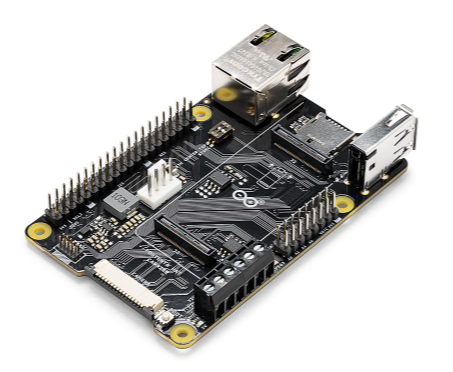
ASX00049

Arduino

* $43.36 - * $50.36

IN STOCK 2847
Buy

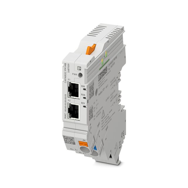
1687559

Phoenix Contact Ltd

[no prices available]

IN STOCK 2
Buy

Reference Designs

RD006

Wurth Elektronik

RD006 - 3 W Dual-output isolated auxiliary supply for communication interfaces and measurement systems

CN0583

Analog Devices Inc.

Multistandard Micropower Verified Smoke Detection System-on-Module

Technical Resources

EVALUATION KITS

EVAL-AD7124-8SDZ

Analog Devices Inc.

$0.00 - * $79.12

IN STOCK 792
Buy
View All