Manufacturer
MORE
Stock

Displaying 61 - 80 of 11965

Evaluation Kits

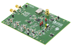
AD9286-500EBZ

Analog Devices Inc.
The AD9286 is an 8-bit, monolithic sampling, analog-to-digital converter (ADC) that supports interleaved operation and is optimized for low cost, low power, and ease of use. Each ADC operates at up to a 250 MSPS conversion rate with outstanding dynamic performance.The AD9286 takes a single sample clock and, with an on-chip clock divider, time interleaves the two ADC cores (each running at one-half the clock frequency) to achieve the rated 500 MSPS. By using the SPI, the user can accurately adjust the timing of the sampling edge per ADC to minimize the image spur energy.The ADC requires a single 1.8 V supply and an encode clock for full performance operation. No external reference components are required for many applications. The digital outputs are LVDS compatible.The AD9286 is available in a Pb-free, 48-lead LFCSP that is specified over the industrial temperature range of ?40?C to +85?C. PRODUCT HIGHLIGHTS Integrated 8-bit, 500 MSPS ADC. Single 1.8 V supply operation with LVDS outputs. Power-down option controlled via a pin-programmable setting.?APPLICATIONS Battery-powered instruments Handheld scope meters Low cost digital oscilloscopes OTS: video over fiber

AD9287-100EBZ

Analog Devices Inc.
The AD9287 is a quad, 8-bit, 100 MSPS analog-to-digital con-verter (ADC) with an on-chip sample-and-hold circuit designedfor low cost, low power, small size, and ease of use. The productoperates at a conversion rate of up to 100 MSPS and is optimized for outstanding dynamic performance and low power in applications where a small package size is critical.The ADC requires a single 1.8 V power supply and LVPECL-/ CMOS-/LVDS-compatible sample rate clock for full performanceoperation. No external reference or driver components arerequired for many applications.The ADC automatically multiplies the sample rate clock for theappropriate LVDS serial data rate. A data clock output (DCO) for capturing data on the output and a frame clock output (FCO) for signaling a new output byte are provided. Individual-channel power-down is supported and typically consumes less than 2 mW when all channels are disabled.The ADC contains several features designed to maximizeflexibility and minimize system cost, such as programmableclock and data alignment and programmable digital test patterngeneration. The available digital test patterns include built-in deterministic and pseudorandom patterns, along with custom user-defined test patterns entered via the serial port interface (SPI).The AD9287 is available in an RoHS compliant, 48-lead LFCSP. It isspecified over the industrial temperature range of ?40?C to +85?C.Product Highlights Small Footprint. Four ADCs are contained in a small, space-saving package. Low power of 133 mW/channel at 100 MSPS. Ease of Use. A data clock output (DCO) is provided that operates at frequencies of up to 400 MHz and supports double data rate (DDR) operation. User Flexibility. The SPI control offers a wide range of flexible features to meet specific system requirements. Pin-Compatible Family. This includes the AD9219 (10-bit), AD9228 (12-bit), and AD9259 (14-bit).ApplicationsMedical imaging and nondestructive ultrasoundPortable ultrasound and digital beam-forming systemsQuadrature radio receiversDiversity radio receiversTape drivesOptical networkingTest equipment

AD9512/PCBZ

Analog Devices Inc.
The AD9512 provides a multi-output clock distribution function for input signals up to 1.6 GHz. The design emphasizes low jitter and low phase noise in order to maximize data converter clocking performance. Three independent LVPECL and two LVDS clock outputs operate to 1.2 GHz and 800 MHz respectively. Optional CMOS clock outputs available to 250 MHz. Each output has a programmable divider, which may be bypassed or set to divide by any integer up to 32.Each divider allows the user to change the phase of one clock output relative to another clock output. This phase select functions as a coarse timing adjustment. One output also features a programmable delay element with a user-selected, fullscale range to 10 ns. This fine tuning delay block is programmed with a 5-bit word, which gives the user 32 possible delays from which to choose.The AD9512 is ideally suited for data converter clocking applications where maximum converter performance is achieved with sub-picosecond jitter encode signals.The AD9512 is available in a 48-lead LFCSP and is specified from -40?C to +85?C. The part may be run from a single 3.3 V supply. ApplicationsLow jitter, low phase noise clock distribution Clocking high speed ADCs, DACs, DDS, DDC, DUC, MxFE? ConvertersWireless infrastructure transceiversHigh performance instrumentationBroadband infrastructure

AD9516-2/PCBZ

Analog Devices Inc.
The AD9516-2?provides a multi-output clock distribution function with subpicosecond jitter performance, along with an on-chip PLL and VCO. The on-chip VCO tunes from 2.05 GHz to 2.33 GHz. Optionally, an external VCO/VCXO of up to 2.4 GHz can be used.The AD9516-2 emphasizes low jitter and phase noise to maximize data converter performance, and it can benefit other applications with demanding phase noise and jitter requirements. The AD9516-2 features six LVPECL outputs (in three pairs) and four LVDS outputs (in two pairs). Each LVDS output can be reconfigured as two CMOS outputs. The LVPECL outputs operate to 1.6 GHz, the LVDS outputs operate to 800 MHz, and the CMOS outputs operate to 250 MHz.Each pair of outputs has dividers that allow both the divide ratio and coarse delay (or phase) to be set. The range of division for the LVPECL outputs is 1 to 32. The LVDS/CMOS outputs allow a range of divisions up to a maximum of 1024.The AD9516-0 is available in a 64-lead LFCSP and can be operated from a single 3.3 V supply. An external VCO, which requires an extended voltage range, can be accommodated by connecting the charge pump supply (VCP) to 5 V. A separate LVPECL power supply can be from 2.5 V to 3.3 V (nominal).The AD9516-2 is specified for operation over the standard industrial range of ?40?C to +85?C.APPLICATIONS Low jitter, low phase noise clock distribution 10/40/100 Gb/sec networking line cards, including SONET, Synchronous Ethernet, OTU2/3/4 Forward error correction (G.710) Clocking high speed ADCs, DACs, DDSs, DDCs, DUCs, MxFEs High performance wireless transceivers ATE and high performance instrumentation

AD9516-4/PCBZ

Analog Devices Inc.
The AD9516-4?provides a multi-output clock distribution function with subpicosecond jitter performance, along with an on-chip PLL and VCO. The on-chip VCO tunes from 1.45 GHz to 1.80 GHz. Optionally, an external VCO/VCXO of up to 2.4 GHz can be used.The AD9516-4 emphasizes low jitter and phase noise to maximize data converter performance, and it can benefit other applications with demanding phase noise and jitter requirements.The AD9516-4 features six LVPECL outputs (in three pairs) and four LVDS outputs (in two pairs). Each LVDS output can be reconfigured as two CMOS outputs. The LVPECL outputs operate to 1.6 GHz, the LVDS outputs operate to 800 MHz, and the CMOS outputs operate to 250 MHz.Each pair of outputs has dividers that allow both the divide ratio and coarse delay (or phase) to be set. The range of division for the LVPECL outputs is 1 to 32. The LVDS/CMOS outputs allow a range of divisions, up to a maximum of 1024.The AD9516-4 is available in a 64-lead LFCSP and can be operated from a single 3.3 V supply. An external VCO, which requires an extended voltage range, can be accommodated by connecting the charge pump supply (VCP to 5 V. A separate LVPECL power supply can be from 2.5 V to 3.3 V (nominal).The AD9516-4 is specified for operation over the industrial range of ?40?C to +85?C.APPLICATIONS Low jitter, low phase noise clock distribution 10/40/100 Gb/sec networking line cards, including SONET, Synchronous Ethernet, OTU2/3/4 Forward error correction (G.710) Clocking high speed ADCs, DACs, DDSs, DDCs, DUCs, MxFEs High performance wireless transceivers ATE and high performance instrumentation?

AD9516-5/PCBZ

Analog Devices Inc.
The AD9516-5?provides a multi-output clock distribution function with subpicosecond jitter performance, along with an on-chip PLL that can be used with an external VCO/VCXO of up to 2.4 GHz.The AD9516-5 emphasizes low jitter and phase noise to maximize data converter performance, and it can benefit otherapplications with demanding phase noise and jitter requirements.The AD9516-5 features six LVPECL outputs (in three pairs)and four LVDS outputs (in two pairs). Each LVDS output canbe reconfigured as two CMOS outputs. The LVPECL outputsoperate to 1.6 GHz, the LVDS outputs operate to 800 MHz, andthe CMOS outputs operate to 250 MHz.Each pair of outputs has dividers that allow both the divide ratio and coarse delay (or phase) to be set. The range of division forthe LVPECL outputs is 1 to 32. The LVDS/CMOS outputs allowa range of divisions up to a maximum of 1024.The AD9516-5 is available in a 64-lead LFCSP and can beoperated from a single 3.3 V supply. An external VCO, which requires an extended voltage range, can be accommodated by connecting the charge pump supply (VCP) to 5.5 V. A separate LVPECL power supply can be from 2.375 V to 3.6 V (nominal).The AD9516-5 is specified for operation over the industrial range of ?40?C to +85?C.For applications requiring an integrated EEPROM, or needing additional outputs, the AD9520-5?and AD9522-5?are available.APPLICATIONS Low jitter, low phase noise clock distribution 10/40/100 Gb/sec networking line cards, including SONET, Synchronous Ethernet, OTU2/3/4 Forward error correction (G.710) Clocking high speed ADCs, DACs, DDSs, DDCs, DUCs, MxFEs High performance wireless transceivers ATE and high performance instrumentation

AD9517-4A/PCBZ

Analog Devices Inc.
The AD9517-4?provides a multi-output clock distribution function with subpicosecond jitter performance, along with an on-chip PLL and VCO. The on-chip VCO tunes from 1.45 GHz to 1.80 GHz. Optionally, an external VCO/VCXO of up to 2.4 GHz can be used.The AD9517-4 emphasizes low jitter and phase noise to maximize data converter performance, and it can benefit other applications with demanding phase noise and jitter requirements.The AD9517-4 features four LVPECL outputs (in two pairs) and four LVDS outputs (in two pairs). Each LVDS output can be reconfigured as two CMOS outputs. The LVPECL outputs operate to 1.6 GHz, the LVDS outputs operate to 800 MHz, and the CMOS outputs operate to 250 MHz.For applications that require additional outputs, a crystal reference input, zero-delay, or EEPROM for automatic configuration at startup, the AD9520 and AD9522 are available. In addition, the AD9516 and AD9518 are similar to the AD9517 but have a different combination of outputs.Each pair of outputs has dividers that allow both the divide ratio and coarse delay (or phase) to be set. The range of division for the LVPECL outputs is 1 to 32. The LVDS/CMOS outputs allow a range of divisions up to a maximum of 1024.The AD9517-4 is available in a 48-lead LFCSP and can be operated from a single 3.3 V supply. An external VCO, which requires an extended voltage range, can be accommodated by connecting the charge pump supply (VCP) to 5 V. A separate LVPECL power supply can be from 2.5 V to 3.3 V (nominal).The AD9517-4 is specified for operation over the industrial range of ?40?C to +85?C.APPLICATIONS Low jitter, low phase noise clock distribution 10/40/100 Gb/sec networking line cards, including SONET, Synchronous Ethernet, OTU2/3/4 Forward error correction (G.710) Clocking high speed ADCs, DACs, DDSs, DDCs, DUCs, MxFEs High performance wireless transceivers ATE and high performance instrumentation

AD9520-2/PCBZ

Analog Devices Inc.
The AD9520-2 provides a multioutput clock distributionfunction with subpicosecond jitter performance, along with anon-chip PLL and VCO. The on-chip VCO tunes from 2.02 GHzto 2.335 GHz. An external 3.3 V/5 V VCO/VCXO of up to 2.4 GHzcan also be used.The AD9520-2 serial interface supports both SPI and I2C?ports.An in-package EEPROM, which can be programmed through theserial interface, can store user-defined register settings forpower-up and chip reset.The AD9520-2 features 12 LVPECL outputs in four groups. Anyof the 1.6 GHz LVPECL outputs can be reconfigured as two250 MHz CMOS outputs. If an application requires LVDSdrivers instead of LVPECL drivers, refer to the AD9522-2.Each group of three outputs has a divider that allows both thedivide ratio (from 1 to 32) and the phase offset or coarse timedelay to be set.The AD9520-2 is available in a 64-lead LFCSP and can be operatedfrom a single 3.3 V supply. The external VCO can have anoperating voltage of up to 5.5 V. A separate output driver powersupply can be from 2.375 V to 3.465 V.The AD9520-2 is specified for operation over the standardindustrial range of ?40?C to +85?C.Applications Low jitter, low phase noise clock distribution Clock generation and translation for SONET, 10Ge, 10GFC, Synchronous Ethernet, OTU2/3/4 Forward error correction (G.710) Clocking high speed ADCs, DACs, DDSs, DDCs, DUCs, MxFEs High performance wireless transceivers ATE and high performance instrumentation Broadband infrastructures

AD9520-3/PCBZ

Analog Devices Inc.
The AD9520-31 provides a multioutput clock distribution function with subpicosecond jitter performance, along with an on-chip PLL and VCO. The on-chip VCO tunes from 1.72 GHz to 2.25 GHz. An external 3.3 V/5 V VCO/VCXO of up to 2.4 GHz can also be used.The AD9520 serial interface supports both SPI and I2C? ports. An in-package EEPROM can be programmed through the serial interface and store user-defined register settings for power-up and chip reset.The AD9520 features 12 LVPECL outputs in four groups. Any of the 1.6 GHz LVPECL outputs can be reconfigured as two 250 MHz CMOS outputs.Each group of outputs has a divider that allows both the divide ratio (from 1 to 32) and the phase (coarse delay) to be set.The AD9520 is available in a 64-lead LFCSP and can be operated from a single 3.3 V supply. The external VCO can have an operating voltage up to 5.5 V. A separate output driver power supply can be from 2.375 V to 3.465 V.The AD9520 is specified for operation over the standard industrial range of ?40?C to +85?C.1The AD9520 is used throughout this data sheet to refer to all the members of the AD9520 family. However, when AD9520-3 is used, it is referring to that specific member of the AD9520 family.Applications Low jitter, low phase noise clock distribution Clock generation and translation for SONET, 10Ge, 10G FC, and other 10 Gbps protocols Forward error correction (G.710) Clocking high speed ADCs, DACs, DDSs, DDCs, DUCs, MxFEs High performance wireless transceivers ATE and high performance instrumentation Broadband infrastructures

AD9522-1/PCBZ

Analog Devices Inc.
The AD9522-11 provides a multioutput clock distribution function with subpicosecond jitter performance, along with an on-chip PLL and VCO. The on-chip VCO tunes from 2.27 GHz to 2.65 GHz. An external 3.3 V/5 V VCO/VCXO of up to 2.4 GHz can also be used.The AD9522 serial interface supports both SPI and I2C? ports. An in-package EEPROM can be programmed through the serial interface and store user-defined register settings for power-up and chip reset.The AD9522 features 12 LVDS outputs in four groups. Any of the 800 MHz LVDS outputs can be reconfigured as two 250 MHz CMOS outputs.Each group of outputs has a divider that allows both the divide ratio (from 1 to 32) and the phase (coarse delay) to be set.The AD9522 is available in a 64-lead LFCSP and can be operated from a single 3.3 V supply. The external VCO can have an operating voltage up to 5.5 V.The AD9522 is specified for operation over the standard industrial range of ?40?C to +85?C.The AD9520-1 is an equivalent part to the AD9522-1 featuring LVPECL/CMOS drivers instead of LVDS/CMOS drivers.1The AD9522 is used throughout this data sheet to refer to all the members of the AD9522 family. However, when AD9522-1 is used, it is referring to that specific member of the AD9522 family.ApplicationsLow jitter, low phase noise clock distributionClock generation and translation for SONET, 10Ge, 10G FC, and other 10 Gbps protocolsForward error correction (G.710)Clocking high speed ADCs, DACs, DDSs, DDCs, DUCs, MxFEsHigh performance wireless transceiversATE and high performance instrumentationBroadband infrastructures

AD9523-1/PCBZ

Analog Devices Inc.
The AD9523-1 provides a low power, multi-output, clock distribution function with low jitter performance, along with an on-chip PLL and VCO with two VCO dividers. The on-chip VCO tunes from 2.94 GHz to 3.1 GHz.The AD9523-1 is designed to support the clock requirements for long term evolution (LTE) and multicarrier GSM base station designs. It relies on an external VCXO to provide the reference jitter cleanup to achieve the restrictive low phase noise requirements necessary for acceptable data converter SNR performance.The input receivers, oscillator, and zero delay receiver provide both single-ended and differential operation. When connected to a recovered system reference clock and a VCXO, the device generates 14 low noise outputs with a range of 1 MHz to 1 GHz, and one dedicated buffered output from the input PLL (PLL1). The frequency and phase of one clock output relative to another clock output can be varied by means of a divider phase select function that serves as a jitter-free, coarse timing adjustment in increments that are equal to half the period of the signal coming out of the VCO.An in-package EEPROM can be programmed through the serial interface to store user-defined register settings for power-up and chip reset.APPLICATIONS LTE and multicarrier GSM base stations Wireless and broadband infrastructure Medical instrumentation Clocking high speed ADCs, DACs, DDSs, DDCs, DUCs, MxFEs Low jitter, low phase noise clock distribution Clock generation and translation for SONET, 10Ge, 10G FC, and other 10 Gbps protocols Forward error correction (G.710) High performance wireless transceivers ATE and high performance instrumentation

AD9559/PCBZ

Analog Devices Inc.
The AD9559 is a low loop bandwidth clock multiplier that provides jitter cleanup and synchronization for many systems, including synchronous optical networks (SONET/SDH). The AD9559 generates an output clock synchronized to up to four external input references. The digital PLL allows for reduction of input time jitter or phase noise associated with the external references. The digitally controlled loop and holdover circuitry of the AD9559 continuously generates a low jitter output clock even when all reference inputs have failed.The AD9559 operates over an industrial temperature range of ?40?C to +85?C. If a single DPLL version of this part is needed, refer to the AD9557.APPLICATIONS Network synchronization, including Synchronous Ethernet and OTN mapping/de-mapping Cleanup of reference clock jitter SONET/SDH clocks up to OC-192, including FEC Stratum 3 holdover, jitter cleanup, and phase transient control Wireless base station controllers Cable infrastructure Data communications

AD9609-20EBZ

Analog Devices Inc.
The AD9609 is a monolithic, single channel 1.8 V supply, 10-bit,20/40/65/80 MSPS analog-to-digital converter (ADC). It featuresa high performance sample-and-hold circuit and on-chip voltagereference.The product uses multistage differential pipeline architecturewith output error correction logic to provide 10-bit accuracy at80 MSPS data rates and to guarantee no missing codes over thefull operating temperature range.The ADC contains several features designed to maximize flexibilityand minimize system cost, such as programmable clock and dataalignment and programmable digital test pattern generation. Theavailable digital test patterns include built-in deterministic andpseudorandom patterns, along with custom user-defined testpatterns entered via the serial port interface (SPI).A differential clock input with selectable internal 1 to 8 divide ratiocontrols all internal conversion cycles. An optional duty cyclestabilizer (DCS) compensates for wide variations in the clock dutycycle while maintaining excellent overall ADC performance.The digital output data is presented in offset binary, gray code, ortwos complement format. A data output clock (DCO) is providedto ensure proper latch timing with receiving logic. Both 1.8 V and3.3 V CMOS levels are supported.The AD9609 is available in a 32-lead RoHS-compliant LFCSPand is specified over the industrial temperature range (?40?Cto +85?C).APPLICATIONS Communications Diversity radio systems Multimode digital receivers GSM, EDGE, W-CDMA, LTE, CDMA2000, WiMAX, TD-SCDMA Smart antenna systems Battery-powered instruments Handheld scope meters Portable medical imaging Ultrasound Radar/LIDAR PET/SPECT imagingPRODUCT HIGHLIGHTS1. The AD9609 operates from a single 1.8 V analog powersupply and features a separate digital output driver supplyto accommodate 1.8 V to 3.3 V logic families.2. The sample-and-hold circuit maintains excellent performancefor input frequencies up to 200 MHz and is designed for lowcost, low power, and ease of use.3. A standard serial port interface supports various productfeatures and functions, such as data output formatting,internal clock divider, power-down, DCO and data output(D9 to D0) timing and offset adjustments, and voltagereference modes.4. The AD9609 is packaged in a 32-lead RoHS compliantLFCSP that is pin compatible with the AD9629 12-bit ADCand the AD9649 14-bit ADC, enabling a simple migrationpath between 10-bit and 14-bit converters sampling from20 MSPS to 80 MSPS.

AD9625-2.0EBZ

Analog Devices Inc.
The AD9625 is a 12-bit monolithic sampling analog-to-digital converter (ADC) that operates at conversion rates of up to 2.6 giga samples per second (GSPS). This product is designed for sampling wide bandwidth analog signals up to the second Nyquist zone. The combination of wide input bandwidth, high sampling rate, and excellent linearity of the AD9625 is ideally suited for spectrum analyzers, data acquisition systems, and a wide assortment of military electronics applications, such as radar and jamming/antijamming measures.The analog input, clock, and SYSREF? signals are differential inputs. The JESD204B-based high speed serialized output is configurable in a variety of one-, two-, four-, six-, or eight-lane configurations. The product is specified over the industrial temperature range of ?40?C to +85?C.PRODUCT HIGHLIGHTS High performance: exceptional SFDR in high sample rate applications, direct RF sampling, and on-chip reference. Flexible digital data output formats based on the JESD204B specification. Control path SPI interface port that supports various product features and functions, such as data formatting, gain, and offset calibration values.APPLICATIONS Spectrum analyzers Military communications Radar High performance digital storage oscilloscopes Active jamming/antijamming Electronic surveillance and countermeasures

AD9625-2.6EBZ

Analog Devices Inc.
The AD9625 is a 12-bit monolithic sampling analog-to-digital converter (ADC) that operates at conversion rates of up to 2.6 giga samples per second (GSPS). This product is designed for sampling wide bandwidth analog signals up to the second Nyquist zone. The combination of wide input bandwidth, high sampling rate, and excellent linearity of the AD9625 is ideally suited for spectrum analyzers, data acquisition systems, and a wide assortment of military electronics applications, such as radar and jamming/antijamming measures.The analog input, clock, and SYSREF? signals are differential inputs. The JESD204B-based high speed serialized output is configurable in a variety of one-, two-, four-, six-, or eight-lane configurations. The product is specified over the industrial temperature range of ?40?C to +85?C.PRODUCT HIGHLIGHTS High performance: exceptional SFDR in high sample rate applications, direct RF sampling, and on-chip reference. Flexible digital data output formats based on the JESD204B specification. Control path SPI interface port that supports various product features and functions, such as data formatting, gain, and offset calibration values.APPLICATIONS Spectrum analyzers Military communications Radar High performance digital storage oscilloscopes Active jamming/antijamming Electronic surveillance and countermeasures

AD9635-125EBZ

Analog Devices Inc.
The AD9635 is a dual, 12-bit, 80 MSPS/125 MSPS analog-to-digital converter (ADC) with an on-chip sample-and-hold circuit designed for low cost, low power, small size, and ease of use. The product operates at a conversion rate of up to 125 MSPS and is optimized for outstanding dynamic performance and low power in applications where a small package size is critical.The ADC requires a single 1.8 V power supply and LVPECL-/ CMOS-/LVDS-compatible sample rate clock for full performanceoperation. No external reference or driver components arerequired for many applications.The ADC automatically multiplies the sample rate clock for theappropriate LVDS serial data rate. A data clock output (DCO) for capturing data on the output and a frame clock output (FCO) forsignaling a new output byte are provided. Individual channelpower-down is supported; the AD9635 typically consumes lessthan 2 mW in the full power-down state. The ADC providesseveral features designed to maximize flexibility and minimize system cost, such as programmable output clock and data alignment and digital test pattern generation. The available digital test patterns include built-in deterministic and pseudorandom patterns, along with custom user-defined test patterns entered via the serial port interface (SPI).The AD9635 is available in a RoHS-compliant, 32-lead LFCSP. It is specified over the industrial temperature range of ?40?Cto +85?C. PRODUCT HIGHLIGHTS Small Footprint. Two ADCs are contained in a small, spacesaving package. Low Power. The AD9635 uses 115 mW/channel at 125 MSPS with scalable power options. Pin Compatibility with the AD9645, a 14-Bit Dual ADC. Ease of Use. A data clock output (DCO) operates at frequencies of up to 500 MHz and supports double data rate (DDR) operation. User Flexibility. The SPI control offers a wide range of flexible features to meet specific system requirements. APPLICATIONS Communications Diversity radio systems Multimode digital receivers GSM, EDGE, W-CDMA, LTE, CDMA2000, WiMAX, TD-SCDMA I/Q demodulation systems Smart antenna systems Broadband data applications Battery-powered instruments Hand held scope meters Portable medical imaging and ultrasound Radar/LIDAR

DC250A-B

Analog Devices Inc.
The LTC1503-1.8/LTC1503-2 are switched capacitor step-down DC/DC converters that produce a regulated output from a 2.4V to 6V input. The parts use switched capacitor fractional conversion to achieve high efficiency over the entire input range. No inductors are required. Internal circuitry controls the step-down conversion ratio to optimize efficiency as the input voltage and load conditions vary. Typical efficiency is 25% higher than that of a low dropout (LDO) linear regulator.Regulation is achieved by sensing the output voltage and enabling the internal switching network as needed to maintain a fixed output voltage. This method of regulation enables the parts to achieve high efficiency at extremely light loads. Low operating current (25?A with no load, 5?A in shutdown) and low external parts count (two 1?F flying capacitors and two 10?F bypass capacitors) make the LTC1503-1.8/LTC1503-2 ideally suited for space constrained battery-powered applications. The parts are fully short-circuit and over temperature protected.The LTC1503-1.8/LTC1503-2 are available in 8-pin MSOP and SO packages.Applications Cellular Phones Handheld Computers Smart Card Readers Low Power DSP Supplies Portable Electronic Equipment Handheld Medical Instruments

DC2520A-B

Analog Devices Inc.
The LTC2344-16 is a 16-bit, low noise 4-channel simulta- neous sampling successive approximation register (SAR) ADC with differential, wide common mode range inputs. Operating from a 5V supply and using the internal reference and buffer, each channel of this SoftSpan? ADC can be independently configured on a conversion-by-conversion basis to accept ?4.096V, 0V to 4.096V, ?2.048V, or 0V to 2.048V signals. Individual channels may also be disabled to increase throughput on the remaining channels.The wide input common mode range and 102dB CMRR of the LTC2344-16 analog inputs allow the ADC to directly digitize a variety of signals, simplifying signal chain design. This input signal flexibility, combined with ?1.25LSB INL, no missing codes at 16 bits, and 93.4dB SNR, makes the LTC2344-16 an ideal choice for many applications requiring wide dynamic range.The LTC2344-16 supports pin-selectable SPI CMOS (1.8V to 5V) and LVDS serial interfaces. Between one and four lanes of data output may be employed in CMOS mode, allowing the user to optimize bus width and throughput.Applications Programmable Logic Controllers Industrial Process Control Medical Imaging High Speed Data Acquisition

LT8652S Demo Board | Dual Channel 8.5A, 18V, Synchronous Step-Down Silent Switcher with 16µA Quiescent Current

Analog Devices Inc.
Demonstration circuit 2523A is an 18V, 8.5A (continuous)/12A (peak) synchronous step-down Silent Switcher® with 16µA quiescent current featuring the LT8652S. The LT8652S is a compact, high efficiency, high speed synchronous monolithic step-down switching with the second generation Silent Switcher structure that minimizes EMI and reduces PCB layout sensitivity. Top and bottom power switches, compensation components and other necessary circuits are inside of the LT8652S to minimize external components and simplify design. The demo board has two outputs: 3.3V and 1.2V from a 3.6V to 18V input. The wide input range allows a variety of input sources, such as automotive batteries and industrial supplies. The SYNC pin on the demo board is grounded by default for low ripple Burst Mode® operation. Move JP2 to FCM without SSM position can change the operation mode to forced continuous mode operation. Once JP2 is on FCM with SSM position, VCC is applied to the SYNC pin for low EMI spread spectrum operation. To synchronous to an external clock, move JP2 to SYNC and apply the external clock to the SYNC turret. The demonstration circuit 2523A runs at 2MHz to minimize solution size. The peak efficiency is 90%. The IC temperature rise is less than 70°C when both channels run at full load, 8.5A each, at 2MHz. The demo board has EMI filters installed for both channels. To use the EMI filter, the input should be tied to VEMI1/VEMI2, not VIN1/VIN2. The LT8652S data sheet gives a complete description of the part, operation and application information. The data sheet must be read in conjunction with this demo manual for DC2523A.

LTM4662 Demo Board | 4.5V ≤ Vin ≤ 20V, Vout1=1.2V@15A, Vout2 = 1.5V@15A

Analog Devices Inc.
Demonstration circuit DC2527A-A features the LTM4662EY, a dual 15A or single 30A high efficiency, switch mode step-down power µModule regulator. The input voltage range is from 4.5V to 20V. With CPWR bias, input voltage can be as low as 2.375V. The output voltage range is 0.6V to 5.5V. Derating is necessary for certain VIN, VOUT, frequency and thermal conditions. The DC2527A-A offers the TRACK/SS pin allowing the user to program output tracking or soft-start period. The board operates in continuous conduction mode in heavy load conditions. For high efficiency at low load currents, the MODE_PLLIN jumper can select discontinuous conduction mode. MODE_PLLIN pin also allows the LTM4662 to synchronize to an external clock signal (between 250kHz and 1MHz). DC2527A-A has the option of choosing both internal and external compensation circuit for LTM4662. Tying the PHASMD pin to different pins generates certain phases of CLKOUT and Channel 2. The LTM4662 data sheet must be read in conjunction with this demo manual prior to working on or modifying demo circuit DC2527A-A.

Displaying 61 - 80 of 11965

Latest Parts

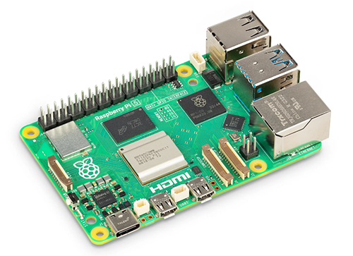
SC1112

Raspberry Pi

$79.61 - $80.00

IN STOCK 13104
Buy

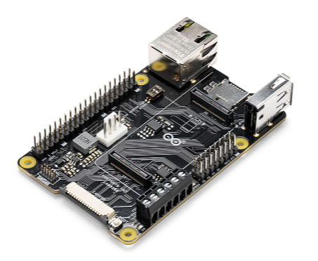
ASX00049

Arduino

* $42.15 - * $45.91

IN STOCK 3111
Buy
IN STOCK 4847
Buy

Reference Designs

RD006

Wurth Elektronik

RD006 - 3 W Dual-output isolated auxiliary supply for communication interfaces and measurement systems

CN0583

Analog Devices Inc.

Multistandard Micropower Verified Smoke Detection System-on-Module

Technical Resources

EVALUATION KITS

EVAL-AD7124-8SDZ

Analog Devices Inc.

$71.95 - * $79.75

IN STOCK 821
Buy
View All