Manufacturer
MORE
Stock

Displaying 101 - 120 of 11821

Evaluation Kits

DC2193A

Analog Devices Inc.
The LT6118 is a complete high side current sense device that incorporates a precision current sense amplifier, an integrated voltage reference and a latching comparator. The comparator latch functionality can be enabled or disabled and the comparator can be configured to reset upon power-on. The input and the open-drain output of the comparator are independent from the current sense amplifier. The comparator trip point and amplifier gain are configured with external resistors.The overall propagation delay of the LT6118 is typically only 1.4?s, allowing for quick reaction to overcurrent conditions. The 1MHz bandwidth allows the LT6118 to be used for error detection in critical applications such as motor control. The high threshold accuracy of the comparator, combined with the ability to latch the comparator, ensures the LT6118 can capture high speed events.The LT6118 is fully specified for operation from ?40?C to 125?C, making it suitable for industrial and automotive applications. The LT6118 is available in the small 8-lead MSOP and 8-lead DFN packages.Applications Overcurrent and Fault Detection Current Shunt Measurement Battery Monitoring Motor Control Automotive Monitoring and Control Industrial Control

DC2199A-B

Analog Devices Inc.
The LTC3766 is a PolyPhase-capable secondary-side controller for synchronous forward converters. When used in conjunction with the LTC3765 active-clamp forward controller and gate driver, the part creates a complete isolated power supply that combines the power of multiphase operation with the speed of secondary-side control.The LTC3766 has been designed to simplify the design of active clamp forward converters. Working in concert with the LTC3765, the LTC3766 forms a robust, self-starting converter that eliminates the need for the separate bias regulator that is commonly used in secondary-side control applications. A precision current-limit coupled with clean start-up into a pre-biased load make the LTC3766 an excellent choice for high-power battery charger applications.The LTC3766 provides extensive remote sensing and output protection features, while Direct Flux Limit guarantees no transformer saturation without compromising transient response. A linear regulator controller and internal bypass LDO are also provided to simplify the generation of the secondary-side bias voltage.Applications Isolated 48V Telecommunication Systems Isolated Battery Chargers Automotive and Military Systems Industrial, Avionics and Heavy Equipment

DC2199B-C

Analog Devices Inc.
The LTC3766 is a PolyPhase-capable secondary-side controller for synchronous forward converters. When used in conjunction with the LTC3765 active-clamp forward controller and gate driver, the part creates a complete isolated power supply that combines the power of multiphase operation with the speed of secondary-side control.The LTC3766 has been designed to simplify the design of active clamp forward converters. Working in concert with the LTC3765, the LTC3766 forms a robust, self-starting converter that eliminates the need for the separate bias regulator that is commonly used in secondary-side control applications. A precision current-limit coupled with clean start-up into a pre-biased load make the LTC3766 an excellent choice for high-power battery charger applications.The LTC3766 provides extensive remote sensing and output protection features, while Direct Flux Limit guarantees no transformer saturation without compromising transient response. A linear regulator controller and internal bypass LDO are also provided to simplify the generation of the secondary-side bias voltage.Applications Isolated 48V Telecommunication Systems Isolated Battery Chargers Automotive and Military Systems Industrial, Avionics and Heavy Equipment

DC2211A

Analog Devices Inc.
The LTC2983 measures a wide variety of temperature sensors and digitally outputs the result, in ?C or ?F, with 0.1?C accuracy and 0.001?C resolution. The LTC2983 can measure the temperature of virtually all standard (type B, E, J, K, N, S, R, T) or custom thermocouples, automatically compensate for cold junction temperatures and linearize the results. The device can also measure temperature with standard 2-, 3- or 4-wire RTDs, thermistors and diodes. It has 20 reconfigurable analog inputs enabling many sensor connections and configuration options. The LTC2983 includes excitation current sources and fault detection circuitry appropriate for each type of temperature sensor.The LTC2983 allows direct interfacing to ground referenced sensors without the need for level shifters, negative supply voltages, or external amplifiers. All signals are buffered and simultaneously digitized with three high accuracy, 24-bit ?? ADCs, driven by an internal 10ppm/?C (maximum) reference.Applications Direct Thermocouple Measurements Direct RTD Measurements Direct Thermistor Measurements Custom Sensor Applications

DC2212A

Analog Devices Inc.
The LTC2983 measures a wide variety of temperature sensors and digitally outputs the result, in ?C or ?F, with 0.1?C accuracy and 0.001?C resolution. The LTC2983 can measure the temperature of virtually all standard (type B, E, J, K, N, S, R, T) or custom thermocouples, automatically compensate for cold junction temperatures and linearize the results. The device can also measure temperature with standard 2-, 3- or 4-wire RTDs, thermistors and diodes. It has 20 reconfigurable analog inputs enabling many sensor connections and configuration options. The LTC2983 includes excitation current sources and fault detection circuitry appropriate for each type of temperature sensor.The LTC2983 allows direct interfacing to ground referenced sensors without the need for level shifters, negative supply voltages, or external amplifiers. All signals are buffered and simultaneously digitized with three high accuracy, 24-bit ?? ADCs, driven by an internal 10ppm/?C (maximum) reference.Applications Direct Thermocouple Measurements Direct RTD Measurements Direct Thermistor Measurements Custom Sensor Applications

LTC3877 Demo Board | Dual Buck Controller, Sub-mΩ DCR Sensing, 6V ≤ VIN ≤ 14V, VOUT1 is VID Programmable from 0.6V to 1.23V @ 30A, VOUT2 is 1.5V @ 30A

Analog Devices Inc.
Demonstration circuits 2229A-A and 2229A-B feature the LTC3877 in two high output current, high efficiency, VID programmed step-down converters with sub-mΩ DCR sensing. For both converters, the input voltage range is 6V to 14V and the switching frequency is 400kHz.

AD9609-20EBZ

Analog Devices Inc.
The AD9609 is a monolithic, single channel 1.8 V supply, 10-bit,20/40/65/80 MSPS analog-to-digital converter (ADC). It featuresa high performance sample-and-hold circuit and on-chip voltagereference.The product uses multistage differential pipeline architecturewith output error correction logic to provide 10-bit accuracy at80 MSPS data rates and to guarantee no missing codes over thefull operating temperature range.The ADC contains several features designed to maximize flexibilityand minimize system cost, such as programmable clock and dataalignment and programmable digital test pattern generation. Theavailable digital test patterns include built-in deterministic andpseudorandom patterns, along with custom user-defined testpatterns entered via the serial port interface (SPI).A differential clock input with selectable internal 1 to 8 divide ratiocontrols all internal conversion cycles. An optional duty cyclestabilizer (DCS) compensates for wide variations in the clock dutycycle while maintaining excellent overall ADC performance.The digital output data is presented in offset binary, gray code, ortwos complement format. A data output clock (DCO) is providedto ensure proper latch timing with receiving logic. Both 1.8 V and3.3 V CMOS levels are supported.The AD9609 is available in a 32-lead RoHS-compliant LFCSPand is specified over the industrial temperature range (?40?Cto +85?C).APPLICATIONS Communications Diversity radio systems Multimode digital receivers GSM, EDGE, W-CDMA, LTE, CDMA2000, WiMAX, TD-SCDMA Smart antenna systems Battery-powered instruments Handheld scope meters Portable medical imaging Ultrasound Radar/LIDAR PET/SPECT imagingPRODUCT HIGHLIGHTS1. The AD9609 operates from a single 1.8 V analog powersupply and features a separate digital output driver supplyto accommodate 1.8 V to 3.3 V logic families.2. The sample-and-hold circuit maintains excellent performancefor input frequencies up to 200 MHz and is designed for lowcost, low power, and ease of use.3. A standard serial port interface supports various productfeatures and functions, such as data output formatting,internal clock divider, power-down, DCO and data output(D9 to D0) timing and offset adjustments, and voltagereference modes.4. The AD9609 is packaged in a 32-lead RoHS compliantLFCSP that is pin compatible with the AD9629 12-bit ADCand the AD9649 14-bit ADC, enabling a simple migrationpath between 10-bit and 14-bit converters sampling from20 MSPS to 80 MSPS.

AD9625-2.0EBZ

Analog Devices Inc.
The AD9625 is a 12-bit monolithic sampling analog-to-digital converter (ADC) that operates at conversion rates of up to 2.6 giga samples per second (GSPS). This product is designed for sampling wide bandwidth analog signals up to the second Nyquist zone. The combination of wide input bandwidth, high sampling rate, and excellent linearity of the AD9625 is ideally suited for spectrum analyzers, data acquisition systems, and a wide assortment of military electronics applications, such as radar and jamming/antijamming measures.The analog input, clock, and SYSREF? signals are differential inputs. The JESD204B-based high speed serialized output is configurable in a variety of one-, two-, four-, six-, or eight-lane configurations. The product is specified over the industrial temperature range of ?40?C to +85?C.PRODUCT HIGHLIGHTS High performance: exceptional SFDR in high sample rate applications, direct RF sampling, and on-chip reference. Flexible digital data output formats based on the JESD204B specification. Control path SPI interface port that supports various product features and functions, such as data formatting, gain, and offset calibration values.APPLICATIONS Spectrum analyzers Military communications Radar High performance digital storage oscilloscopes Active jamming/antijamming Electronic surveillance and countermeasures

AD9625-2.6EBZ

Analog Devices Inc.
The AD9625 is a 12-bit monolithic sampling analog-to-digital converter (ADC) that operates at conversion rates of up to 2.6 giga samples per second (GSPS). This product is designed for sampling wide bandwidth analog signals up to the second Nyquist zone. The combination of wide input bandwidth, high sampling rate, and excellent linearity of the AD9625 is ideally suited for spectrum analyzers, data acquisition systems, and a wide assortment of military electronics applications, such as radar and jamming/antijamming measures.The analog input, clock, and SYSREF? signals are differential inputs. The JESD204B-based high speed serialized output is configurable in a variety of one-, two-, four-, six-, or eight-lane configurations. The product is specified over the industrial temperature range of ?40?C to +85?C.PRODUCT HIGHLIGHTS High performance: exceptional SFDR in high sample rate applications, direct RF sampling, and on-chip reference. Flexible digital data output formats based on the JESD204B specification. Control path SPI interface port that supports various product features and functions, such as data formatting, gain, and offset calibration values.APPLICATIONS Spectrum analyzers Military communications Radar High performance digital storage oscilloscopes Active jamming/antijamming Electronic surveillance and countermeasures

AD9635-125EBZ

Analog Devices Inc.
The AD9635 is a dual, 12-bit, 80 MSPS/125 MSPS analog-to-digital converter (ADC) with an on-chip sample-and-hold circuit designed for low cost, low power, small size, and ease of use. The product operates at a conversion rate of up to 125 MSPS and is optimized for outstanding dynamic performance and low power in applications where a small package size is critical.The ADC requires a single 1.8 V power supply and LVPECL-/ CMOS-/LVDS-compatible sample rate clock for full performanceoperation. No external reference or driver components arerequired for many applications.The ADC automatically multiplies the sample rate clock for theappropriate LVDS serial data rate. A data clock output (DCO) for capturing data on the output and a frame clock output (FCO) forsignaling a new output byte are provided. Individual channelpower-down is supported; the AD9635 typically consumes lessthan 2 mW in the full power-down state. The ADC providesseveral features designed to maximize flexibility and minimize system cost, such as programmable output clock and data alignment and digital test pattern generation. The available digital test patterns include built-in deterministic and pseudorandom patterns, along with custom user-defined test patterns entered via the serial port interface (SPI).The AD9635 is available in a RoHS-compliant, 32-lead LFCSP. It is specified over the industrial temperature range of ?40?Cto +85?C. PRODUCT HIGHLIGHTS Small Footprint. Two ADCs are contained in a small, spacesaving package. Low Power. The AD9635 uses 115 mW/channel at 125 MSPS with scalable power options. Pin Compatibility with the AD9645, a 14-Bit Dual ADC. Ease of Use. A data clock output (DCO) operates at frequencies of up to 500 MHz and supports double data rate (DDR) operation. User Flexibility. The SPI control offers a wide range of flexible features to meet specific system requirements. APPLICATIONS Communications Diversity radio systems Multimode digital receivers GSM, EDGE, W-CDMA, LTE, CDMA2000, WiMAX, TD-SCDMA I/Q demodulation systems Smart antenna systems Broadband data applications Battery-powered instruments Hand held scope meters Portable medical imaging and ultrasound Radar/LIDAR

AD9648-125EBZ

Analog Devices Inc.
The AD9648 is a monolithic, dual-channel, 1.8 V supply, 14-bit, 105 MSPS/125 MSPS analog-to-digital converter (ADC). It features a high performance sample-and-hold circuit and on-chip voltage reference. The product uses multistage differential pipeline architecture with output error correction logic to provide 14-bit accuracy at 125 MSPS data rates and to guarantee no missing codes over the full operating temperature range.The ADC contains several features designed to maximize flexibility and minimize system cost, such as programmable clock and data alignment and programmable digital test pattern generation. The available digital test patterns include built-in deterministic and pseudorandom patterns, along with custom user-defined test patterns entered via the serial port interface (SPI).A differential clock input controls all internal conversion cycles. An optional duty cycle stabilizer (DCS) compensates for wide variations in the clock duty cycle while maintaining excellent overall ADC performance.The digital output data is presented in offset binary, Gray code, or twos complement format. A data output clock (DCO) is provided for each ADC channel to ensure proper latch timing with receiving logic. Output logic levels of 1.8 V CMOS or LVDS are supported. Output data can also be multiplexed onto a single output bus.The AD9648 is available in a 64-lead RoHS compliant LFCSP and is specified over the industrial temperature range (?40?C to +85?C). Applications Communications Diversity radio systems Multimode digital receivers GSM, EDGE, W-CDMA, LTE, CDMA2000, WiMAX, TD-SCDMA I/Q demodulation systems Smart antenna systems Broadband data applications Battery-powered instruments Hand held scope meters Portable medical imaging Ultrasound Radar/LIDARProduct Highlights The AD9648 operates from a single 1.8 V analog power supply and features a separate digital output driver supply to accommodate 1.8 V CMOS or LVDS logic families. The patented sample-and-hold circuit maintains excellent performance for input frequencies up to 200 MHz and is designed for low cost, low power, and ease of use. A standard serial port interface supports various product features and functions, such as data output formatting, internal clock divider, power-down, DCO/data timing and offset adjustments. The AD9648 is packaged in a 64-lead RoHS compliant LFCSP that is pin compatible with the AD9650/AD9269/AD9268 16-bit ADC?s, the AD9258 14-bit ADC, the AD9628/AD9231 12-bit ADC?s, and the AD9608/AD9204 10-bit ADC?s, enabling a simple migration path between 10-bit and 16-bit converters sampling from 20 MSPS to 125 MSPS.

AD9649-80EBZ

Analog Devices Inc.
The AD9649 is a monolithic, single channel 1.8 V supply, 14-bit, 20/40/65/80 MSPS analog-to-digital converter (ADC). It features a high performance sample-and-hold circuit and an on-chip volt-age reference.The product uses multistage differential pipeline architecture with output error correction logic to provide 14-bit accuracy at 80 MSPS data rates and to guarantee no missing codes over the full operating temperature range.The ADC contains several features designed to maximize flexibility and minimize system cost, such as programmable clock and data alignment and programmable digital test pattern generation. The available digital test patterns include built-in deterministic and pseudorandom patterns, along with custom user-defined test patterns entered via the serial port interface (SPI).A differential clock input with optional 1, 2, or 4 divide ratios controls all internal conversion cycles.The digital output data is presented in offset binary, gray code, or twos complement format. A data output clock (DCO) is provided to ensure proper latch timing with receiving logic. Both 1.8 V and 3.3 V CMOS levels are supported.The AD9649 is available in a 32-lead RoHS-compliant LFCSP and is specified over the industrial temperature range (?40?C to +85?C).PRODUCT HIGHLIGHTS The AD9649 operates from a single 1.8 V analog power supply and features a separate digital output driver supply to accommodate 1.8 V to 3.3 V logic families. The sample-and-hold circuit maintains excellent performance for input frequencies up to 200 MHz and is designed for low cost, low power, and ease of use. A standard serial port interface (SPI) supports various product features and functions, such as data output formatting, internal clock divider, power-down, DCO, data output (D13 to D0) timing and offset adjustments, and voltage reference modes. The AD9649 is packaged in a 32-lead RoHS-compliant LFCSP that is pin compatible with the AD9629 12-bit ADC and the AD9609 10-bit ADC, enabling a simple migration path between 10-bit and 14-bit converters sampling from 20 MSPS to 80 MSPS.?APPLICATIONS Communications Diversity radio systems Multimode digital receivers GSM, EDGE, W-CDMA, LTE, CDMA2000, WiMAX, TD-SCDMA Smart antenna systems Battery-powered instruments Handheld scope meters Portable medical imaging Ultrasound Radar/LIDAR

AD9680-1000EBZ

Analog Devices Inc.
The AD9680 is a dual, 14-bit, 1.25 GSPS/1 GSPS/820 MSPS/500 MSPS analog-to-digital converter (ADC). The device has an on-chip buffer and sample-and-hold circuit designed for low power, small size, and ease of use. This device is designed for sampling wide bandwidth analog signals of up to 2 GHz. The AD9680 is optimized for wide input bandwidth, high sampling rate, excellent linearity, and low power in a small package.The dual ADC cores feature a multistage, differential pipelined architecture with integrated output error correction logic. Each ADC features wide bandwidth inputs supporting a variety of user-selectable input ranges. An integrated voltage reference eases design considerations.The analog input and clock signals are differential inputs. Each ADC data output is internally connected to two digital down-converters (DDCs). Each DDC consists of up to five cascaded signal processing stages: a 12-bit frequency translator (NCO), and four half-band decimation filters. The DDCs are bypassed by default.In addition to the DDC blocks, the AD9680 has several functions that simplify the automatic gain control (AGC) function in the communications receiver. The programmable threshold detector allows monitoring of the incoming signal power using the fast detect output bits of the ADC. If the input signal level exceeds the programmable threshold, the fast detect indicator goes high. Because this threshold indicator has low latency, the user can quickly turn down the system gain to avoid an overrange condition at the ADC input.Users can configure the Subclass 1 JESD204B-based high speed serialized output in a variety of one-, two-, or four-lane configurations, depending on the DDC configuration and the acceptable lane rate of the receiving logic device. Multiple device synchronization is supported through the SYSREF? and SYNCINB? input pins.The AD9680 has flexible power-down options that allow significant power savings when desired. All of these features can be programmed using a 1.8 V to 3.3 V capable, 3-wire SPI.The AD9680 is available in a Pb-free, 64-lead LFCSP and is specified over the ?40?C to +85?C industrial temperature range. This product is protected by a U.S. patent.PRODUCT HIGHLIGHTS Wide full power bandwidth supports IF sampling of signals up to 2 GHz. Buffered inputs with programmable input termination eases filter design and implementation. Four integrated wideband decimation filters and numerically controlled oscillator (NCO) blocks supporting multiband receivers. Flexible serial port interface (SPI) controls various product features and functions to meet specific system requirements. Programmable fast overrange detection. 9 mm ? 9 mm, 64-lead LFCSP.APPLICATIONS Communications Diversity multiband, multimode digital receivers 3G/4G, TD-SCDMA, W-CDMA, GSM, LTE General-purpose software radios Ultrawideband satellite receivers Instrumentation Radars Signals intelligence (SIGINT) DOCSIS 3.0 CMTS upstream receive paths HFC digital reverse path receivers

AD9680-1250EBZ

Analog Devices Inc.
The AD9680 is a dual, 14-bit, 1.25 GSPS/1 GSPS/820 MSPS/500 MSPS analog-to-digital converter (ADC). The device has an on-chip buffer and sample-and-hold circuit designed for low power, small size, and ease of use. This device is designed for sampling wide bandwidth analog signals of up to 2 GHz. The AD9680 is optimized for wide input bandwidth, high sampling rate, excellent linearity, and low power in a small package.The dual ADC cores feature a multistage, differential pipelined architecture with integrated output error correction logic. Each ADC features wide bandwidth inputs supporting a variety of user-selectable input ranges. An integrated voltage reference eases design considerations.The analog input and clock signals are differential inputs. Each ADC data output is internally connected to two digital down-converters (DDCs). Each DDC consists of up to five cascaded signal processing stages: a 12-bit frequency translator (NCO), and four half-band decimation filters. The DDCs are bypassed by default.In addition to the DDC blocks, the AD9680 has several functions that simplify the automatic gain control (AGC) function in the communications receiver. The programmable threshold detector allows monitoring of the incoming signal power using the fast detect output bits of the ADC. If the input signal level exceeds the programmable threshold, the fast detect indicator goes high. Because this threshold indicator has low latency, the user can quickly turn down the system gain to avoid an overrange condition at the ADC input.Users can configure the Subclass 1 JESD204B-based high speed serialized output in a variety of one-, two-, or four-lane configurations, depending on the DDC configuration and the acceptable lane rate of the receiving logic device. Multiple device synchronization is supported through the SYSREF? and SYNCINB? input pins.The AD9680 has flexible power-down options that allow significant power savings when desired. All of these features can be programmed using a 1.8 V to 3.3 V capable, 3-wire SPI.The AD9680 is available in a Pb-free, 64-lead LFCSP and is specified over the ?40?C to +85?C industrial temperature range. This product is protected by a U.S. patent.PRODUCT HIGHLIGHTS Wide full power bandwidth supports IF sampling of signals up to 2 GHz. Buffered inputs with programmable input termination eases filter design and implementation. Four integrated wideband decimation filters and numerically controlled oscillator (NCO) blocks supporting multiband receivers. Flexible serial port interface (SPI) controls various product features and functions to meet specific system requirements. Programmable fast overrange detection. 9 mm ? 9 mm, 64-lead LFCSP.APPLICATIONS Communications Diversity multiband, multimode digital receivers 3G/4G, TD-SCDMA, W-CDMA, GSM, LTE General-purpose software radios Ultrawideband satellite receivers Instrumentation Radars Signals intelligence (SIGINT) DOCSIS 3.0 CMTS upstream receive paths HFC digital reverse path receivers

AD9684-500EBZ

Analog Devices Inc.
The AD9684 is a dual, 14-bit, 500 MSPS ADC. The device has an on-chip buffer and a sample-and-hold circuit designed for low power, small size, and ease of use. This product is designed for sampling wide bandwidth analog signals. The AD9684 is optimized for wide input bandwidth, a high sampling rate, excellent linearity, and low power in a small package.The dual ADC cores feature a multistage, differential pipelined architecture with integrated output error correction logic. Each ADC features wide bandwidth buffered inputs, supporting a variety of user selectable input ranges. An integrated voltage reference eases design considerations. Each ADC data output is internally connected to an optional decimate by 2 block.The analog input and clock signals are differential inputs. Each ADC data output is internally connected to two digital downconverters (DDCs). Each DDC consists of four cascaded signal processing stages: a 12-bit frequency translator (NCO), and three half-band decimation filters supporting a divide by factor of two, four, and eight.Applications Communications Diversity multi-band, multi-mode digital receivers 3G/4G, TD-SCDMA, WCDMA, MC-GSM, LTE General-purpose software radios Ultrawideband satellite receiver Instrumentation (spectrum analyzers, network analyzers, integrated RF test solutions) Radar Digital oscilloscopes High speed data acquisition systems DOCSIS CMTS upstream receive paths HFC digital reverse path receivers

AD9689-2600EBZ

Analog Devices Inc.
The AD9689 is a dual, 14-bit, 2.0 GSPS/2.6 GSPS analog-to-digital converter (ADC). The device has an on-chip buffer and a sample-and-hold circuit designed for low power, small size, and ease of use. This product is designed to support communications applications capable of direct sampling wide bandwidth analog signals of up to 5 GHz. The ?3 dB bandwidth of the ADC input is 9 GHz. The AD9689 is optimized for wide input bandwidth, high sampling rate, excellent linearity, and low power in a small package.The dual ADC cores feature a multistage, differential pipelined architecture with integrated output error correction logic. Each ADC features wide bandwidth inputs supporting a variety of user-selectable input ranges. An integrated voltage reference eases design considerations. The analog input and clock signals are differential inputs. The ADC data outputs are internally connected to four digital downconverters (DDCs) through a crossbar mux. Each DDC consists of multiple cascaded signal processing stages: a 48-bit frequency translator (numerically controlled oscillator (NCO)), and decimation rates. The NCO has the option to select preset bands over the general-purpose input/output (GPIO) pins, which enables the selection of up to three bands. Operation of the AD9689 between the DDC modes is selectable via SPI-programmable profiles.In addition to the DDC blocks, the AD9689 has several functions that simplify the automatic gain control (AGC) function in a communications receiver. The programmable threshold detector allows monitoring of the incoming signal power using the fast detect control bits in Register 0x0245 of the ADC. If the input signal level exceeds the programmable threshold, the fast detect indicator goes high. Because this threshold indicator has low latency, the user can quickly turn down the system gain to avoid an overrange condition at the ADC input. In addition to the fast detect outputs, the AD9689 also offers signal monitoring capability. The signal monitoring block provides additional information about the signal being digitized by the ADC.The user can configure the Subclasss 1 JESD204B-based high speed serialized output in a variety of one-lane, two-lane, four-lane, and eight-lane configurations, depending on the DDC configuration and the acceptable lane rate of the receiving logic device. Multidevice synchronization is supported through the SYSREF? and SYNCINB? input pins.The AD9689 has flexible power-down options that allow significant power savings when desired. All of these features can be programmed using a 3-wire serial port interface (SPI).The AD9689 is available in a Pb-free, 196-ball BGA, specified over the ?40?C to +85?C ambient temperature range. This product is protected by a U.S. patent.Note that throughout this data sheet, multifunction pins, such as FD_A/GPIO_A0, are referred to either by the entire pin name or by a single function of the pin, for example, FD_A, when only that function is relevant.Product Highlights Wide, input ?3 dB bandwidth of 9 GHz supports direct radio frequency (RF) sampling of signals up to about 5 GHz. Four integrated, wideband decimation filters and NCO blocks supporting multiband receivers. Fast NCO switching enabled through the GPIO pins. SPI controls various product features and functions to meet specific system requirements. Programmable fast overrange detection and signal monitoring. On-chip temperature diode for system thermal management. 12 mm ? 12 mm, 196-ball BGA. Pin, package, feature, and memory map compatible with the AD9208 14-bit, 3.0 GSPS, JESD204B dual ADC.Applications Diversity multiband and multimode digital receivers 3G/4G, TD-SCDMA, W-CDMA, and GSM, LTE, LTE-A Electronic test and measurement systems Phased array radar and electronic warfare DOCSIS 3.0 CMTS upstream receive paths HFC digital reverse path receivers

AD9705-DPG2-EBZ

Analog Devices Inc.
The AD9704/AD9705/AD9706/AD9707 are the fourth-generation family in the TxDAC series of high performance, CMOS digital-to-analog converters (DACs). This pin-compatible, 8-/10-/12-/14-bit resolution family is optimized for low power operation, while maintaining excellent dynamic performance. The AD9704/AD9705/AD9706/AD9707 family is pin-compatible with the AD9748/AD9740/AD9742/AD9744 family of TxDAC converters and is specifically optimized for the transmit signal path of communication systems. All of the devices share the same interface, LFCSP package, and pinout, providing an upward or downward component selection path based on performance, resolution, and cost. The AD9704/AD9705/AD9706/AD9707 offers exceptional ac and dc performance, while supporting update rates up to 175 MSPS.The flexible power supply operating range of 1.7 V to 3.6 V and low power dissipation of the AD9704/AD9705/AD9706/AD9707 parts make them well suited for portable and low power applications.Power dissipation of the AD9704/AD9705/AD9706/AD9707 can be reduced to 15 mW, with a small trade-off in performance, by lowering the full-scale current output. In addition, a power-down mode reduces the standby power dissipation to approximately 2.2 mW.The AD9704/AD9705/AD9706/AD9707 has an optional serial peripheral interface (SPI?) that provides a higher level of programmability to enhance performance of the DAC. An adjustable output, common-mode feature allows for easy interfacing to other components that require common modes from 0 V to 1.2 V.Edge-triggered input latches and a 1.0 V temperature-compensated band gap reference have been integrated to provide a complete, monolithic DAC solution. The digital inputs support 1.8 V and 3.3 V CMOS logic families.PRODUCT HIGHLIGHTS Pin Compatible. The AD9704/AD9705/AD9706/AD9707 line of TxDAC?converters is pin-compatible with theAD9748/AD9740/AD9742/AD9744 TxDAC line (LFCSP package). Low Power. Complete CMOS DAC operates on a single supply of 3.6 V down to 1.7 V, consuming 50 mW (3.3 V) and 12 mW (1.8 V). The DAC full-scale current can be reduced for lower power operation. Sleep and power-down modes are provided for low power idle periods. Self-Calibration. Self-calibration enables true 14-bit INL and DNL performance in the AD9707. Twos Complement/Binary Data Coding Support. Data input supports twos complement or straight binary data coding. Flexible Clock Input. A selectable high speed, single-ended,and differential CMOS clock input supports 175 MSPS conversion rate. Device Configuration. Device can be configured through pin strapping, and SPI control offers a higher level of programmability. Easy Interfacing to Other Components. Adjustable common-mode output allows for easy interfacing to other signal chain components that accept common-mode levels from 0 V to 1.2 V. On-Chip Voltage Reference. The AD9704/AD9705/AD9706/AD9707 include a 1.0 V temperature-compensated band gap voltage reference. Industry-Standard 32-Lead LFCSP Package.

AD9715-DPG2-EBZ

Analog Devices Inc.
The AD9714/AD9715/AD9716/AD9717 are pin-compatible, dual, 8-/10-/12-/14-bit, low power digital-to-analog converters (DACs) that provide a sample rate of 125 MSPS. These TxDAC? converters are optimized for the transmit signal path of communication systems. All the devices share the same interface, package, and pinout, providing an upward or downward component selection path based on performance, resolution, and cost.The AD9714/AD9715/AD9716/AD9717 offer exceptional ac and dc performance and support update rates up to 125 MSPS.The flexible power supply operating range of 1.8 V to 3.3 V and low power dissipation of the AD9714/AD9715/AD9716/AD9717 make them well-suited for portable and low power applications.PRODUCT HIGHLIGHTS Low Power. DACs operate on a single 1.8 V to 3.3 V supply; total power consumption reduces to 35 mW at 125 MSPS with a 1.8 V supply. Sleep and power-down modes are provided for low power idle periods. CMOS Clock Input. High speed, single-ended CMOS clock input supports a 125 MSPS conversion rate. Easy Interfacing to Other Components. Adjustable output common mode from 0 V to 1.2 V allows easy interfacing to other components that accept common- mode levels greater than 0 V.?APPLICATIONS Wireless infrastructures Picocell, femtocell base stations Medical instrumentation Ultrasound transducer excitation Portable instrumentation Signal generators, arbitrary waveform generators

AD9717-DPG2-EBZ

Analog Devices Inc.
The AD9714/AD9715/AD9716/AD9717 are pin-compatible, dual, 8-/10-/12-/14-bit, low power digital-to-analog converters (DACs) that provide a sample rate of 125 MSPS. These TxDAC? converters are optimized for the transmit signal path of communication systems. All the devices share the same interface, package, and pinout, providing an upward or downward component selection path based on performance, resolution, and cost.The AD9714/AD9715/AD9716/AD9717 offer exceptional ac and dc performance and support update rates up to 125 MSPS.The flexible power supply operating range of 1.8 V to 3.3 V and low power dissipation of the AD9714/AD9715/AD9716/AD9717 make them well-suited for portable and low power applications.PRODUCT HIGHLIGHTS Low Power. DACs operate on a single 1.8 V to 3.3 V supply; total power consumption reduces to 35 mW at 125 MSPS with a 1.8 V supply. Sleep and power-down modes are provided for low power idle periods. CMOS Clock Input. High speed, single-ended CMOS clock input supports a 125 MSPS conversion rate. Easy Interfacing to Other Components. Adjustable output common mode from 0 V to 1.2 V allows easy interfacing to other components that accept common- mode levels greater than 0 V.?APPLICATIONS Wireless infrastructures Picocell, femtocell base stations Medical instrumentation Ultrasound transducer excitation Portable instrumentation Signal generators, arbitrary waveform generators

AD9737A-EBZ

Analog Devices Inc.
The AD9737A/AD9739A are 11-bit and 14-bit, 2.5 GSPS high performance RF DACs that are capable of synthesizing wideband signals from dc up to 3 GHz. The AD9737A/AD9739A are pin and functionally compatible with the AD9739 with the exception that the AD9737A/AD9739A do not support synchronization or RZ mode, and are specified to operate between 1.6 GSPS and 2.5 GSPS. By elimination of the synchronization circuitry, some nonideal artifacts such as images and discrete clock spurs remain stationary on the AD9737A/AD9739A between power-up cycles, thus allowing for possible system calibration. AC linearity and noise performance remain the same between the AD9739 and the AD9737A/AD9739A.The inclusion of on-chip controllers simplifies system integration. A dual-port, source synchronous, LVDS interface simplifies the digital interface with existing FGPA/ASIC technology. On-chip controllers are used to manage external and internal clock domain variations over temperature to ensure reliable data transfer from the host to the DAC core. A serial peripheral interface (SPI) is used for device configuration as well as readback of status registers.The AD9737A/AD9739A are manufactured on a 0.18 ?m CMOS process and operate from 1.8 V and 3.3 V supplies. They are supplied in a 160-ball chip scale ball grid array for reduced package parasitics.Product Highlights Ability to synthesize high quality wideband signals with bandwidths of up to 1.25 GHz in the first or second Nyquist zone. A proprietary quad-switch DAC architecture provides exceptional ac linearity performance while enabling mixmode operation. A dual-port, double data rate, LVDS interface supports the maximum conversion rate of 2500 MSPS. On-chip controllers manage external and internal clock domain skews. Programmable differential current output with an 8.66 mA to 31.66 mA range.Applications Broadband communications systems DOCSIS CMTS systems Military jammers Instrumentation, automatic test equipment Radar, avionics

Displaying 101 - 120 of 11821

Latest Parts

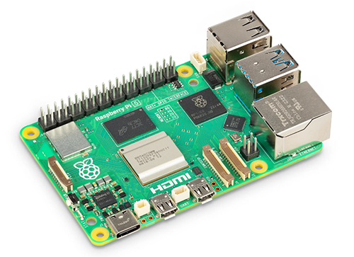
SC1112

Raspberry Pi

$79.61 - $86.40

IN STOCK 10294
Buy

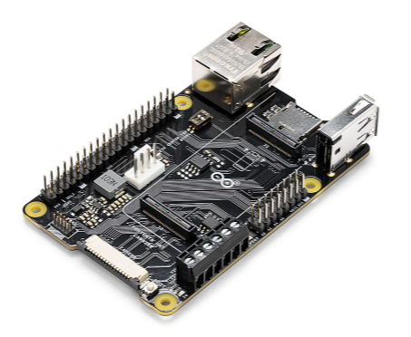
ASX00049

Arduino

* $39.45 - * $44.37

IN STOCK 3132
Buy

AD96685BRZ

Analog Devices Inc.

$1.72 - * $11.78

IN STOCK 4921
Buy

Reference Designs

RD006

Wurth Elektronik

RD006 - 3 W Dual-output isolated auxiliary supply for communication interfaces and measurement systems

CN0583

Analog Devices Inc.

Multistandard Micropower Verified Smoke Detection System-on-Module

Technical Resources

EVALUATION KITS

EVAL-AD7124-8SDZ

Analog Devices Inc.

$73.86 - * $75.91

IN STOCK 808
Buy
View All