KSZ8999-EVAL
Microchip Technology Inc.Ethernet Development Tools KSZ899 Eval, No Power Supply Incl.
89KTT0816AP
Renesas Electronics CorporationEvaluation Board for 89HT0816AP Retimer, 8-lane, 8Gbps, PCIe3
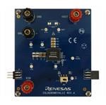
ISL8280MEVAL1Z
Renesas Electronics CorporationPower Management IC Development Tools ISL8280M EVAL BOARD 1, 10A,12V Single Channel 12 x11 HDA MO
EVALSTDRV600HB8
STMicroelectronicsPower Management IC Development Tools INDUSTRIAL & POWER CONVERSION
KSZ8765CLX-EVAL
Microchip Technology Inc.Ethernet Development Tools 5-Port 10/100 with RGMII/GMII + Fiber - Evaluation Board
KSZ8999-EVAL
Microchip Technology Inc.Ethernet Development Tools KSZ899 Eval, No Power Supply Incl.
KSZ8795CLXD-EVAL
Microchip Technology Inc.Ethernet Development Tools 5-Port 10/100 with RGMII/GMII - Evaluation Board
KSZ8851SNL-EVAL
Microchip Technology Inc.Ethernet Development Tools Single Ethernet Port + SPI Bus Interface Eval Board
KSZ8873MLL-EVAL
Microchip Technology Inc.Ethernet Development Tools 3-Port Fast Ethernet Switch with 1x MII Interface - Evaluation Board
KSZ8795CLXD-EVAL
Microchip Technology Inc.Ethernet Development Tools 5-Port 10/100 with RGMII/GMII - Evaluation Board
EVALSTDRIVE601
STMicroelectronicsPower Management IC Development Tools INDUSTRIAL & POWER CONVERSION

KSZ8999-EVAL
Microchip Technology Inc.KSZ8999 Ethernet Controller (PHY and MAC) Interface Evaluation Board
KSZ9031MNX-EVAL
Microchip Technology Inc.Ethernet Development Tools 1-Port Gigabit Ethernet PHY - Evaluation Board
KSZ8091RNA-EVAL
Microchip Technology Inc.Ethernet Development Tools Eval - 10/100 PHY w/EEE & WOL, 0.11u
KSZ8795CLXD-EVAL
Microchip Technology Inc.KSZ8795CLX Ethernet Controller (PHY and MAC) Interface Evaluation Board
KSZ8851SNL-EVAL
Microchip Technology Inc.Ethernet Development Tools Single Ethernet Port + SPI Bus Interface Eval Board
KSZ9031MNX-EVAL
Microchip Technology Inc.Ethernet Development Tools 1-Port Gigabit Ethernet PHY - Evaluation Board
KSZ8795CLXD-EVAL
Microchip Technology Inc.Ethernet Development Tools 5-Port 10/100 with RGMII/GMII - Evaluation Board


