
LTC2266-12 | 12-Bit, 80Msps, 1.8V Dual Serial ADC, 5MHz < AIN < 170MHz, Requires DC1371 and DC1075
Analog Devices Inc.DC1532A-I: Demo Board for the LTC2266-12 12-Bit, 80Msps Low Power Dual ADCs.
DC1532A-J
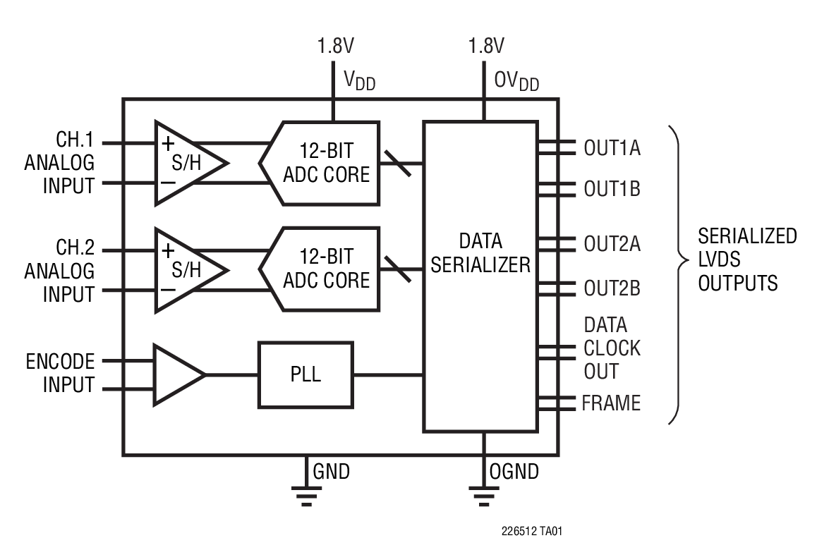
Analog Devices Inc.The LTC2265-12/LTC2264-12/LTC2263-12 are 2-channel, simultaneous sampling 12-bit A/D converters designed for digitizing high frequency, wide dynamic range signals. They are perfect for demanding communications applications with AC performance that includes 71dB SNR and 90dB spurious free dynamic range (SFDR). Ultralow jitter of 0.15psRMS allows undersampling of IF frequencies with excellent noise performance.DC specs include ?0.3LSB INL (typ), ?0.1LSB DNL (typ) and no missing codes over temperature. The transition noise is a low 0.3LSBRMS.The digital outputs are serial LVDS to minimize the number of data lines. Each channel outputs two bits at a time (2-lane mode) or one bit at a time (1-lane mode). The LVDS drivers have optional internal termination and adjustable output levels to ensure clean signal integrity.The ENC+ and ENC? inputs may be driven differentially or single-ended with a sine wave, PECL, LVDS, TTL, or CMOS inputs. An internal clock duty cycle stabilizer allows high performance at full speed for a wide range of clock duty cycles. Bits LTC2265-12 12 LTC2265-14 14 Applications Communications Cellular Base Stations Software Defined Radios Portable Medical Imaging Multichannel Data Acquisition Nondestructive Testing
LTC2264-12 | 12-Bit, 40Msps, 1.8V Dual Serial ADC, 5MHz < AIN < 170MHz, Requires DC1371 and DC1075
Analog Devices Inc.DC1532A-K: Demo Board for the LTC2264-1212-Bit, 40Msps Low Power Dual ADCs.

LT3596EUHG Demo Board | LED Driver, 6V ≤ VIN ≤ 55V, Output = 8 Series LEDs at 100mA
Analog Devices Inc.DC1542A: Demo Board for LT3596 60V Step-Down LED Driver.

DC1563A-G
Analog Devices Inc.The LTC2313-14 is a 14-bit, 2.5Msps, serial sampling A/D converter that draws only 5mA from a single 3V or 5V supply. The LTC2313-14 contains an integrated low drift reference and reference buffer providing a low cost, high performance (20ppm/?C maximum) and space saving solution. The LTC2313-14 achieves outstanding AC performance of 77dB SINAD and ?85dB THD while sampling at 2.5Msps. The extremely high sample rate-topower ratio makes the LTC2313-14 ideal for compact, low power, high speed systems. The supply current decreases at lower sampling rates as the device automatically enters nap mode after conversions.The LTC2313-14 has a high speed SPI-compatible serial interface that supports 1.8V, 2.5V, 3V and 5V logic. The fast 2.5Msps throughput with no cycle latency makes the LTC2313-14 ideally suited for a wide variety of high speed applications.? Bits LTC2313-12 12 LTC2313-14 14 Applications Communication Systems High Speed Data Acquisition Handheld Terminal Interface Medical Imaging Uninterrupted Power Supplies Battery Operated Systems Automotive

LT3760 Demo Board | 8-Channel Boost LED Driver, 20V ≤ VIN ≤ 28V, VLED = 55V @ 100mA
Analog Devices Inc.DC1573A is an 8-Channel High Voltage Boost LED Driver featuring the LT3760. The LT3760 drives up to 100mA per string and has a maximum LED string voltage of 45V. The VIN terminal is powered from an 10V to 14V input supply and is distinct from the 24V PVIN supply (20V to 28V) for best thermal performance. Overvoltage protection is set at 55V in case the LEDs are removed from the circuit. If the LEDs are opened, the FAULT terminal output flag goes low and reports the fault condition. If one or more of the 8 LED channels is not used, its LED pin or terminal should be tied to VOUT (LED+) to disable it. Multiple channels can be tied in parallel by tying their LED1-LED8 pins together.

LT3083EQ Demo Board | Single Resistor Prog Low Dropout Linear Regulator, 1.7V ≤ VIN ≤ 23V, VOUT = 1.2V/1.5V/1.8V/2.5V/3.3V/5.0V @ 3A
Analog Devices Inc.Demonstration circuit 1585A is an adjustable 3A linear regulator featuring the LT3083 in the DD-PAK-5 package. Architected as a precision current source and voltage follower, the LT3083 can be used in many applications requiring high current, adjustability to zero output, and no heat sink. Internal protection circuitry includes current limiting and thermal limiting.The device brings out the collector of the pass transistor to allow low dropout operation when used with multiple supplies.
The demo board oprerates with an input supply voltage range of 1.7V to 23V. A control voltage bias supply that is 1.2V to 1.4V higher than the input voltage is required for proper regulation. A key feature of the LT3083 is its wide output voltage range. The DC1585A's jumper-selectable output voltage can be set to 1.2V, 1.5V, 1.8V, 2.5V, 3.3V, 5.0V, or a user-selectable value. DC1585A can be used as a high current linear regulator, a post regulator for switching supplies, a variable voltage supply or a low output voltage power supply.


