
DC513A
Analog Devices Inc.The LTC2846 is a 3-driver/3-receiver multiprotocol transceiver with on-chip cable termination. When combined with the LTC2844 or LTC2845, this chip set forms a complete software-selectable DTE or DCE interface port that supports the RS232, RS449, EIA530, EIA530-A, V.35, V.36 and X.21 protocols. All necessary cable termination is provided inside the LTC2846. The LTC2846 has a boost regulator that takes in a 3.3V input and switches at 1.2MHz, allowing the use of tiny, low cost capacitors and inductors 2mm or less in height.The 5V output drives an internal charge pump that requires only five space-saving surface mounted capacitors. The LTC2846 is available in a 36-lead SSOP surface mount package.Applications Data Networking CSU and DSU Data Routers

LTC5508ESC6 | 7GHz RF Power Detector
Analog Devices Inc.DC539A: Demo Board for the LTC5508 300MHz to 7GHz RF Power Detector with Buffered Output in SC70 Package.

LTC3723EGN-1 Demo Board | Isolated Supply, 36V ≤ VIN ≤ 72V, VOUT1 = 3.3V @ 40A, VOUT2 = 2.5V @ 10A
Analog Devices Inc.Demonstration circuit 541A is an isolated synchronous push-pull converter featuring the LTC3723-1, LTC3901, LT1431 and LT3710. The design provides an isolated 3.3V at 40A and 2.5V at 10A from a 48V telecom (36V to 72V) input voltage. Isolation voltage is 1500VDC.
The demo board also can provide 3.3V @ 50A with the 2.5V output disabled.

DC544A
Analog Devices Inc.The LT1934 is a micropower step-down DC/DC converter with internal 400mA power switch, packaged in a low profile (1mm) ThinSOT. With its wide input range of 3.2V to 34V, the LT1934 can regulate a wide variety of power sources, from 4-cell alkaline batteries and 5V logic rails to unregulated wall transformers and lead-acid batteries. Quiescent current is just 12?A and a zero current shutdown mode disconnects the load from the input source, simplifying power management in battery-powered systems. Burst Mode? operation and the low drop internal power switch result in high efficiency over a broad range of load current.The LT1934 provides up to 300mA of output current. The LT1934-1 has a lower current limit, allowing optimum choice of external components when the required output current is less than 60mA. Fast current limiting protects the LT1934 and external components against shorted outputs, even at 34V input.Applications Wall Transformer Regulation Automotive Battery Regulation Standby Power for Portable Products Distributed Supply Regulation Industrial Control Supplies

LT3460ESC6 | 1.3MHz Boost and SEPIC DC/DC Converter in SC70, Boost = 5VIN, SEPIC = 10V~16VIN, VOUT = 12V at 50mA/70mA
Analog Devices Inc.Demonstration circuit 545 features the LT3460, step-up DC/DC converter with 1.3MHz constant frequency in a SC70 package. There are two switching regulator circuits in DC545. The 12V output boost converter (upper circuit) is designed to convert 5V input to 12V output at 70mA of load current and the SEPIC converter (lower circuit) is designed to convert 10V ~ 16V input to 12V at 50mA.

LTC2920 Single (-1) & Dual (-2) Margining Controller
Analog Devices Inc.DC563A: Demo Board for the LTC2920 Single (-1) & Dual (-2) Margining Controller.

LTC3421EUF | VIN = 1.8V to 3.2V, VOUT = 3.3V @ 1A
Analog Devices Inc.Demonstration Circuit 565 is a constant-frequency synchronous boost converter using the LTC3421. Guaranteed to start-up at 1V input voltage, this converter provides up to 95% efficiency. For 1.8V minimum input voltage, this converter can provide up to 1A load current. This converter has true output disconnect by eliminating body diode conduction of the internal PMOS rectifier. The output voltage is set at 3.3V. A different output voltage in the range of 2.4V to 5.25V can be obtained by changing one of the feedback resistors.

DC567A
Analog Devices Inc.The LTC4053 is a standalone linear charger for lithium-ion batteries that can be powered directly from a USB port. The IC contains an on-chip power MOSFET and eliminates the need for an external sense resistor and blocking diode. Thermal regulation automatically adjusts charge current to limit die temperature during high power or high ambient temperature conditions. This feature protects the end product and the LTC4053 from thermal stress while the IC charges the battery at maximum rate without interruption.The charge current and charge time can be set externally with a single resistor and capacitor, respectively. When the input supply (wall adapter or USB supply) is removed, the LTC4053 automatically enters a low current sleep mode, dropping the battery drain current to less than 5?A.The LTC4053 also includes NTC temperature sensing, C/10 detection circuitry, AC present logic, low battery charge conditioning (trickle charging) and shutdown (25?A supply current).The LTC4053 is available in a 10-pin thermally enhanced MSOP package.Applications Cellular Telephones Handheld Computers Charging Docks and Cradles MP3 Players Digital Cameras

DC627A-A
Analog Devices Inc.The LT3461/LT3461A are general purpose fixed frequency current mode step-up DC/DC converters. Both devices feature an integrated Schottky and a low VCESAT switch allowing a small converter footprint and lower parts cost. The LT3461 switches at 1.3MHz while the LT3461A switches at 3MHz. These high switching frequencies enable the use of tiny, low cost and low height capacitors and inductors. The constant switching frequency results in predictable output noise that is easy to filter, and the inductor based topology ensures an input free from switching noise typically present with charge pump solutions. The high voltage switch in the LT3461/LT3461A is rated at 40V making the device ideal for boost converters up to 38V.The LT3461/LT3461A are available in a low profile (1mm) SOT-23 package. Switching Frequency LT3461 1.3MHz LT3461A 3MHz Applications Digital Cameras CCD Bias Supply XDSL Power Supply TFT-LCD Bias Supply Local 5V or 12V Supply Medical Diagnostic Equipment Battery Backup
DC627A-B
Analog Devices Inc.The LT3461/LT3461A are general purpose fixed frequency current mode step-up DC/DC converters. Both devices feature an integrated Schottky and a low VCESAT switch allowing a small converter footprint and lower parts cost. The LT3461 switches at 1.3MHz while the LT3461A switches at 3MHz. These high switching frequencies enable the use of tiny, low cost and low height capacitors and inductors. The constant switching frequency results in predictable output noise that is easy to filter, and the inductor based topology ensures an input free from switching noise typically present with charge pump solutions. The high voltage switch in the LT3461/LT3461A is rated at 40V making the device ideal for boost converters up to 38V.The LT3461/LT3461A are available in a low profile (1mm) SOT-23 package. Switching Frequency LT3461 1.3MHz LT3461A 3MHz Applications Digital Cameras CCD Bias Supply XDSL Power Supply TFT-LCD Bias Supply Local 5V or 12V Supply Medical Diagnostic Equipment Battery Backup

DC638A
Analog Devices Inc.The LT1725 is a monolithic switching regulator controller specifically designed for the isolated flyback topology. It drives the gate of an external MOSFET and is generally powered from a third transformer winding. These features allow for an application input voltage limited only by external power path components. The third transformer winding also provides output voltage feedback information, such that an optoisolator is not required. Its gate drive capability coupled with a suitable external MOSFET can deliver load power up to tens of watts.The LT1725 has a number of features not found on most other switching regulator ICs. By utilizing current mode switching techniques, it provides excellent AC and DC line regulation. Its unique control circuitry can maintain regulation well into discontinuous mode in most applications. Optional load compensation circuitry allows for improved load regulation. An optional undervoltage lockout pin halts operation when the application input voltage is too low. An optional external capacitor implements a soft-start function. A 3V output is available at up to several mA for powering primary side application circuitry.Applications Telecom Isolated Converters Offline Isolated Power Supplies Instrumentation Power Supplies

DC651A
Analog Devices Inc.The LT5522 active downconverting mixer is optimized for high linearity downconverter applications including cable and wireless infrastructure. The IC includes a high speed differential LO buffer amplifier driving a double-balanced mixer. The LO buffer is internally matched for wideband, single-ended operation with no external components.The RF input port incorporates an integrated RF transformer and is internally matched over the 1.2GHz to 2.3GHz frequency range with no external components. The RF input match can be shifted down to 600MHz, or up to 2.7GHz, with a single shunt capacitor or inductor, respectively. The high level of integration minimizes the total solution cost, board space and system-level variation.The LT5522 delivers high performance and small size without excessive power consumption.*Operation over a wider frequency range is possible with reduced performance. Consult factory for information and assistance.Applications Cellular, PCS and UMTS Band Infrastructure CATV Downlink Infrastructure 2.4GHz ISM High Linearity Downmixer Applications

LTC3802EGN Demo Board | Dual, VIN = 7V to 24V, VOUT1 = 3.3V @ 15A, VOUT2 = 2.5V @ 15A
Analog Devices Inc.Demonstration circuit 653A is a dual 15A step-down DC/DC converter featuring the LTC3802EGN. The LTC3802EGN itself is a synchronous voltage mode controller. Output #1 of demonstration circuit 653A is a 3.3V / 15A rail and output #2 is a 2.5V / 15A rail. The input voltage range is 7V to 24V.The nominal switching frequency of the LTC3802 is 550kHz and its phase lockable synchronization range is 330kHz to 750kHz.

LT1568 Fourth Order Active RC Filter IC
Analog Devices Inc.Demonstration circuit DC675C is for the evaluation of filter circuits using an LT1568. The LT1568 is a dual 2nd order active-RCfilterbuildingblockwithprecision ±0.75% capacitors and low noise op amps with 180MHz GBW trimmed to ±10% maximum variation. The ±10% GBW variation of the LT1568 op amps allows for minimizing the higher frequency error by decreasing resistor values. The cutoff or center frequency (fC) range of an LT1568 filter is 200kHz to 10MHz (5MHz for a bandpass filter). The low limit of 200kHz was chosen only to minimize resistor noise and DC offsets (using external capacitors the fC frequency can be less than 200kHz).
For testing and evaluation, the DC675C assembly is configured as a single 4th order, 500kHz narrow passband bandpass filter.
For other possible LT1568 configurations, the DC675C has unused pads for 0805 surface mount resistors and capacitors preconfigured with PCB traces to allow for the following high accuracy LT1568 filter circuits:
4th order lowpass filter
5th order lowpass filter
4th order narrow passband bandpass
4th order wide passband bandpass
4th order highpass filter
Refer to the LT1568 data sheet for additional information about filter circuit configurations.

LT1952-1EGN-1, LTC3900ES Demo Board | VIN=36V-75V, VOUT=3.3V @ 50A
Analog Devices Inc.DC677A: Demo Board for the LTC3900 Synchronous Rectifier Driver for Forward Converters.
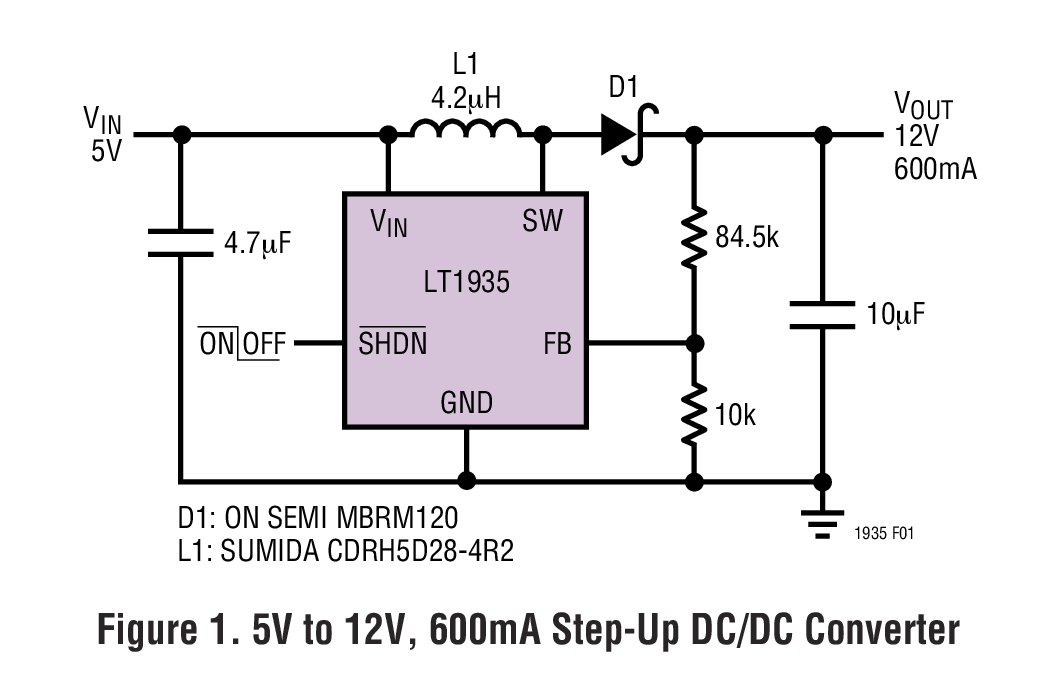
LT1935ES5 Demo Board | 3.3V to 5.5V Input, VOUT = 12V at up to 600mA
Analog Devices Inc.Demonstration circuit DC683 features LT1935 1.2MHz boost DC/DC converter with a 2A switch. The demo board is designed to generate 12V output from a 3.3V to 5.5V input voltage range and can provide 600mA at 12V from a 5V input.

LT1943EFE | 4-Output Switching Regulator For TFT-LCD Panels, VIN = 4.5V - 8V, VOUT = 3.3V @ 1.5A, 13V @ 500mA, 30V @ 20mA, -10V @ 50mA
Analog Devices Inc.DC697A: Demo Board for the LT1943 High Current Quad Output Regulator for TFT LCD Panels.
LTC4053EMSE-4.2 | Li-Ion Battery Charger, VIN = 4.25V to 6.3V, Bat = 4.2V @ 0.5A/1A
Analog Devices Inc.DC705A: Demo Board for the LTC4053-4.2 USB Compatible Lithium-Ion Battery Charger with Thermal Regulation.

LTC4557EUD | Dual SIM Card Power Supply and Interface
Analog Devices Inc.DC709A: Demo Board for the LTC4557 Dual SIM/Smart Card Power Supply and Interface.

LTC3738CUHF Demo Board | 3-Phase, 8V ≤ VIN ≤ 14V, VOUT = VRM9.X/10.X @ 65A
Analog Devices Inc.Demonstration circuits 721A-A and 721A-B are high current step-down converters for Intel VRM/VRD10 and VRM9 processor power applications. The 6-phase DC721A-A features two current-mode PolyPhaseTM controllers, the LTC3738CUHF (3-Phase Buck Controller for Intel VRM9/VRM10 with Active Voltage Positioning and the the LTC3731CUH (3-Phase, 600kHz, Synchronous Buck Switching Regulator Controller). and provides up to 120A output current. The DC721A-B is a single LTC3738 3-phase 65A output supply. The input voltage range for both demo boards is from 8V to 14V, and the output voltage is controlled by the VID setting.


