MAX22164CAEE+
Part Number : MAX22164CAEE+
Analog Devices Inc.DIGITAL ISOLATOR, 200MBPS, 6CH, QSOP-16;
MAX22666CAWE+
Part Number : MAX22666CAWE+
Analog Devices Inc.DIGITAL ISOLATOR, 200MBPS, 6CH, WSOIC-16;
CABLE-PH16
Part Number : CABLE-PH16
Analog Devices Inc.16 Position Cable Assembly Rectangular Plug to Individual Wire Leads 0.656' (200.00mm, 7.87")
F-440-1
Part Number : F-440-1
Analog Devices Inc.RF IC VCO/PLL Synthesizer General Purpose 62.5MHz ~ 8GHz Down Converter 80-LGA (18x18)
LTC1773EMS
Part Number : LTC1773EMS
Analog Devices Inc.Buck Regulator Positive Output Step-Down DC-DC Controller IC 10-MSOP
LTC2642ACDD-16
Part Number : LTC2642ACDD-16
Analog Devices Inc.16 Bit Digital to Analog Converter 1 10-DFN (3x3)


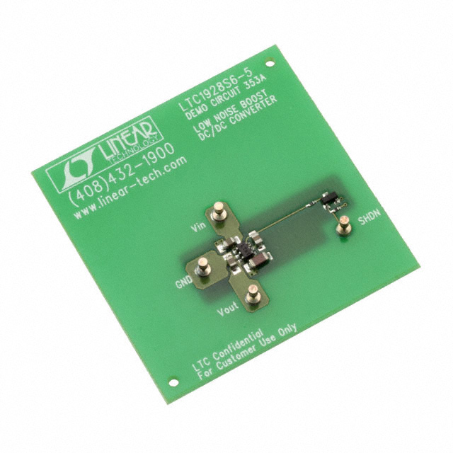
LTC1928-5
Part Number : LTC1928-5
Analog Devices Inc.LTC1928-5 - DC/DC, Step Up with LDO 1, Non-Isolated Outputs Evaluation Board
MAX6326UR31+T
Part Number : MAX6326UR31+T
Analog Devices Inc.Supervisory Circuits 3-Pin, Ultra-Low-Power SC70/SOT P Reset Circuits
LTC2975IUP
Part Number : LTC2975IUP
Analog Devices Inc.Power Supply Controller Power Supply Controller/Monitor 64-QFN (9x9)
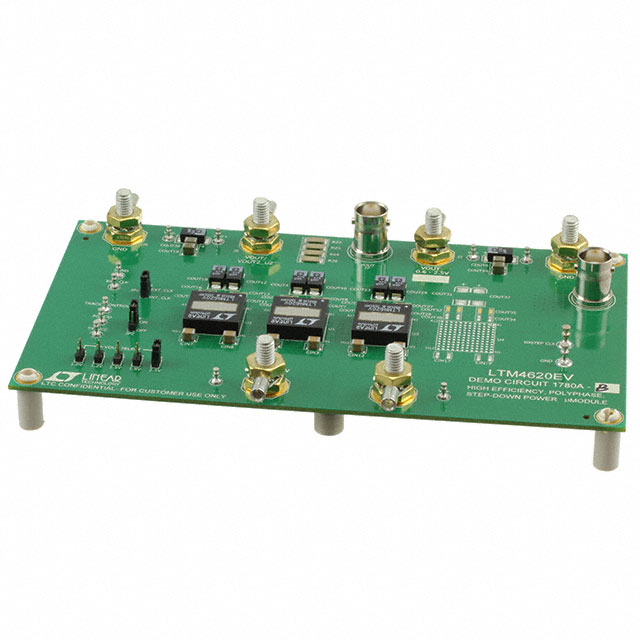
1780AB
Part Number : 1780AB
Analog Devices Inc.LTM4620 µModule® DC/DC, Step Down 1, Non-Isolated Outputs Evaluation Board
LTM4616IY#PBF
Part Number : LTM4616IY#PBF
Analog Devices Inc.Switching Voltage Regulators 2x 8A per Ch L VIN DC/DC uModule Reg

LTC1629EG-6
Part Number : LTC1629EG-6
Analog Devices Inc.Buck Regulator Positive Output Step-Down DC-DC Controller IC 28-SSOP

LTC3863IMSE
Part Number : LTC3863IMSE
Analog Devices Inc.Buck Regulator Positive or Negative Output Step-Down DC-DC Controller IC 12-MSOP-EP
LTC2974IUP
Part Number : LTC2974IUP
Analog Devices Inc.Power Supply Controller Monitor, Sequencer, Supervisor 64-QFN (9x9)
DS2401P+T&R
Part Number : DS2401P+T&R
Analog Devices Inc.Security ICs / Authentication ICs Silicon Serial Number
LTC3425EUH
Part Number : LTC3425EUH
Analog Devices Inc.Boost Switching Regulator IC Positive Adjustable 2.4V 1 Output 5A (Switch) 32-WFQFN Exposed Pad


