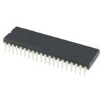
DS3930E
Part Number : DS3930E
Analog Devices Inc.Digital Potentiometer ICs HEX NON VOLATILE POT WITH I/O & MEM
ICL7662EBA
Part Number : ICL7662EBA
Analog Devices Inc.Switching Voltage Regulators CMOS Voltage Converter

LTC3569EUD
Part Number : LTC3569EUD
Analog Devices Inc.Buck Switching Regulator IC Positive Adjustable 0.425V 3 Output 600mA, 1.2A 20-WFQFN Exposed Pad
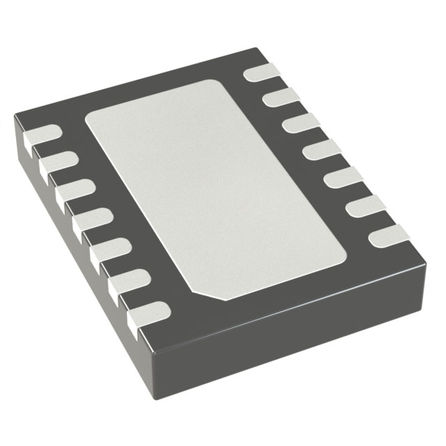
LTC3851EUD
Part Number : LTC3851EUD
Analog Devices Inc.Buck Regulator Positive Output Step-Down DC-DC Controller IC 16-QFN (3x3)
LTC3424
Part Number : LTC3424
Analog Devices Inc.Boost Switching Regulator IC Positive Adjustable 1.5V 1 Output 2A (Switch) 10-TFSOP, 10-MSOP (0.118", 3.00mm Width)

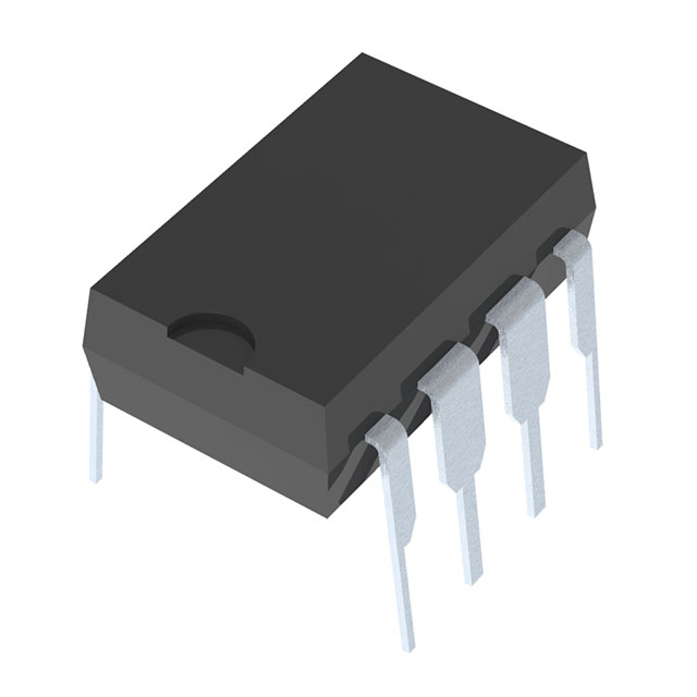
MAX4326ESA
Part Number : MAX4326ESA
Analog Devices Inc.General Purpose Amplifier 2 Circuit Rail-to-Rail 8-SOIC

ICM7212AMIPL+
Part Number : ICM7212AMIPL+
Analog Devices Inc.LED Display Drivers Four Digit Display Decoder/Drivers
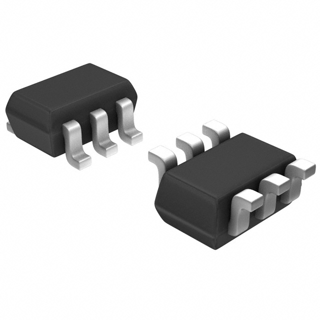
LTC6752HSC6-1
Part Number : LTC6752HSC6-1
Analog Devices Inc.Comparator General Purpose CMOS SC-70-6

LTC1294
Part Number : LTC1294
Analog Devices Inc.Data Acquisition System (DAS), ADC 12 b 46.5k Serial, Parallel 20-SO

LTC2493
Part Number : LTC2493
Analog Devices Inc.24 Bit Analog to Digital Converter 2, 4 Input 1 Sigma-Delta 14-DFN (4x3)

866A
Part Number : 866A
Analog Devices Inc.LED Driver IC 9 Output DC DC Regulator Switched Capacitor (Charge Pump) I2C, PWM Dimming 25mA 20-LFCSP (4x4)


LTC2960IDC-1
Part Number : LTC2960IDC-1
Analog Devices Inc.Supervisor Open Drain or Open Collector 2 Channel 8-DFN (2x2)
MAX1765
Part Number : MAX1765
Analog Devices Inc.Linear Voltage Regulator IC Positive Adjustable 1 Output 100mA TSOT-23-6
LTC1983ES6-3
Part Number : LTC1983ES6-3
Analog Devices Inc.Charge Pump Switching Regulator IC Negative Fixed -3V 1 Output 100mA SOT-23-6 Thin, TSOT-23-6
LTC2311HMSE-12
Part Number : LTC2311HMSE-12
Analog Devices Inc.12 Bit Analog to Digital Converter 1 Input 1 SAR 16-MSOP-EP

LTC3631EMS8E-5
Part Number : LTC3631EMS8E-5
Analog Devices Inc.Buck Switching Regulator IC Positive or Negative Fixed 5V 1 Output 100mA 8-TSSOP, 8-MSOP (0.118", 3.00mm Width) Exposed Pad


