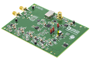
EV1HMC6787ALC5A
Analog Devices Inc.The HMC6787ALC5A is a compact GaAs MMIC I/Q variable gain upconverter in a leadless RoHS compliant SMT package. This device provides a small signal conversion gain of 11 dB with 17 dBc of sideband rejection, and 13 dB of gain control. The HMC6787ALC5A utilizes a RF variable gain amplifier preceded by an I/Q mixer where the LO is driven by a X2 multiplier. IF1 and IF2 mixer inputs are provided and an external 90? hybrid is needed to select the required sideband. The I/Q mixer topology reduces the need for filtering of the unwanted sideband. The HMC6787ALC5A is a much smaller alternative to hybrid style single sideband upconverter assemblies and it eliminates the need for wire bonding by allowing the use of surface mount manufacturing techniques.APPLICATIONS Point-to-Point and Point-to-Multi-Point Radio Military Radar, EW & ELINT Satellite Communications Sensors

EV1HMC6789BLC5A
Analog Devices Inc.The HMC6789BLC5A is a compact GaAs MMIC I/Qdownconverter in a 12-terminal, RoHS compliant,ceramic leadless chip carrier (LCC) package. Thisdevice provides a small signal conversion gain of 14 dBwith 25 dBc of image rejection. The HMC6789BLC5Autilizes a low noise amplifier to drive the I/Q mixerwhere the LO is driven by a ?2 multiplier. IF1 and IF2mixer inputs are provided and an external 90? hybridis needed to select the required sideband. The I/Qmixer topology reduces the need for filtering of theunwanted sideband. The HMC6789BLC5A is a muchsmaller alternative to hybrid style single sidebanddownconverter assemblies and it eliminates the needfor wire bonding by allowing the use of surface mountmanufacturing techniques.Applications Point-to-Point and Point-to-Multi-Point Radios Military Radar, EW & ELINT Satellite Communications Sensors

EV1HMC6832ALP5L
Analog Devices Inc.The HMC6832 is an input selectable, 2:8 differential fanoutbuffer designed for low noise clock distribution. The IN_SELcontrol pin selects one of the two differential inputs. This inputis then buffered to all eight differential outputs. The low jitteroutputs of the HMC6832 lead to synchronized low noiseswitching of downstream circuits, such as mixers, analog-todigitalconverters (ADCs)/digital-to-analog converters (DACs),or serializer/deserializer (SERDES) devices. The device is capableof low voltage, positive emitter-coupled logic (LVPECL) or lowvoltage differential signaling (LVDS) configurations by pullingthe CONFIG pin low for LVPECL or high or open (internallypulled high) for pseudo LVDS.Product Highlights Multiple Output Configurations. The CONFIG pin allows the user to select LVPECL or LVDS output termination. Multiple Supply Voltage Operation. The HMC6832 operates at 2.5 V or 3.3 V for LVPECL terminations (2.5 V only for LVDS). Low Noise. The HMC6832 noise is low, typically from ?168 dBc/Hz to ?162 dBc/Hz up to 3000 MHz. Low Propagation Delay. The HMC6832 displays a low delay, less than 207 ps, typical. Channel skew is also low, ?5 ps, typical. Low Core Current. The HMC6832 has a low core current of 56 mA, typical. Applications SONET, Fibre Channel, GigE clock distribution ADC/DAC clock distribution Low skew and jitter clocks Wireless/wired communications Level translation High performance instrumentation Medical imaging Single-ended to differential conversions

EV1HMC7545ABLP47
Analog Devices Inc.The HMC7545 is a unidirectional, quad-channel, protocol and data rate agnostic, asynchronous signal conditioner, designed for short and intermediate range optical modules, line cards, and backplane applications operating at up to 14.2 Gbps.Each channel provides programmable input equalization, LOS and receiver detection, automatic output squelch, programmable output swing and output de-emphasis.All high speed differential inputs and outputs of the HMC7545 are current mode logic (CML), terminated on-chip with 50 ??to the positive supply, and can be dc-coupled or ac-coupled.The device uses a single supply, 2.5 V or 3.5 V, and its typical power dissipation is less than 80 mW per channel.The HMC7545 is packaged in a 36-lead, 4 mm ? 7 mm LFCSP package and operates from -40?C to +85?C.Applications QSFP+ direct attach active copper modules 10 Gb, 40 Gb Ethernet and OTN line cards 10 Gb, 40 Gb backplane drivers 8 Gb, 16 Gb Fibre Channel and InfiniBand? EDR line cards and backplane drivers 8 Gb, 10 Gb, 16 Gb active optical modules 8 Gb, 10 Gb, 16 Gb active copper cable assemblies 1.5 Gb, 3 Gb, 6 Gb, 12 Gb SAS/SATA PCIe 1.x, 2.0, 3.0 Broadband and automatic test and measurement

EV1HMC788ALP2
Analog Devices Inc.The HMC788A is a 0.01 GHz to 10 GHz, gain block, monolithic microwave integrated circuit (MMIC) amplifier using gallium arsenide (GaAs), pseudomorphic high electron mobility transistor (pHEMT) technology.This 2 mm ? 2 mm LFCSP amplifier can be used as either a cascadable 50 ? gain stage, or to drive the local oscillator (LO) port of many of the single and double balanced mixers from Analog Devices, Inc. with up to 20 dBm output power.The HMC788A offers 14 dB of gain and an output IP3 of 33 dBm while requiring only 76 mA from a 5 V supply.The Darlington feedback pair exhibits reduced sensitivity to normal process variations and yields excellent gain stability over temperature while requiring a minimal number of external bias components.Applications Cellular, 3G, LTE, WiMAX, and 4G LO driver applications Microwave radio Test and measurement equipment Ultra wideband (UWB) communications

EV1HMC7911LP5
Analog Devices Inc.The HMC7911 is a compact gallium arsenide (GaAs), pseudomorphic(pHEMT), monolithic microwave integrated circuit(MMIC) upconverter in a RoHS compliant, low stress, injectionmolded plastic LFCSP package that operates from 17 GHz to20 GHz. This device provides a small signal conversion gain of18 dB with 30 dBc of sideband rejection. The HMC7911 uses avariable gain amplifier preceded by an in-phase/quadrature (I/Q)mixer that is driven by an active 2? local oscillator (LO) multiplier.IF1 and IF2 mixer inputs are provided, and an external 90? hybridis needed to select the required sideband. The I/Q mixer topologyreduces the need for filtering of the unwanted sideband. TheHMC7911 is a much smaller alternative to hybrid style singlesideband (SSB) upconverter assemblies, and it eliminates theneed for wire bonding by allowing the use of surface-mountmanufacturing techniques.Applications Point to point and point to multipoint radios Military radars, electronic warfare (EW), and electronic intelligence (ELINT) Satellite communications Sensors

EV1HMC7912LP5
Analog Devices Inc.The HMC7912 is a compact, gallium arsenide (GaAs), pseudomorphic(pHEMT), monolithic microwave integrated circuit(MMIC) upconverter in a RoHS compliant, low stress, injectionmolded plastic LFCSP package that operates from 21 GHz to24 GHz. This device provides a small signal conversion gain of15 dB with 22 dBc of sideband rejection. The HMC7912 uses avariable gain amplifier preceded by an in-phase/quadrature (I/Q)mixer that is driven by an active 2? LO multiplier. IF1 and IF2mixer inputs are provided, and an external 90? hybrid is needed toselect the required sideband. The I/Q mixer topology reducesthe need for filtering of the unwanted sideband. The HMC7912is a much smaller alternative to hybrid style single sideband (SSB)upconverter assemblies, and it eliminates the need for wirebonding by allowing the use of surface-mount manufacturingtechniques.Applications Point to point and point to multipoint radios Military radars, electronic warfare (EW), and electronic intelligence (ELINT) Satellite communications Sensors
EV1HMC8073LP3D
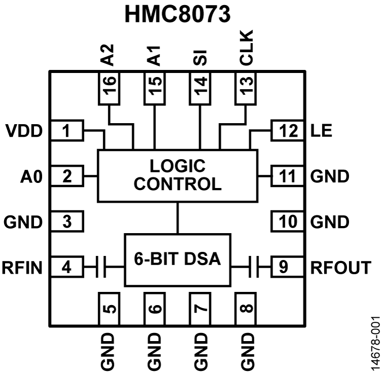
Analog Devices Inc.The HMC8073 is a 6-bit digital step attenuator (DSA), operating from 0.6 GHz to 3.0 GHz, that features 31.5 dB of attenuation range with 0.5 dB steps.The HMC8073 is implemented in a silicon process, offering a fast settling time, low power consumption, and high electrostatic discharge (ESD) robustness. The device features safe state transitions, allowing attenuation state changes without overshooting, and is optimized for excellent step accuracy and high power and high linearity over frequency and temperature range. The radio frequency (RF) input and output are internally matched to 50 ? and do not require any external matching components. The design is bidirectional, and the RF input and output are interchangeable.The external address feature of the HMC8073 allows users to control up to eight DSAs using a single bus. The DSA has an on-chip regulator that supports a wide supply operating range from 3.3 V to 5.0 V with no performance change in electrical characteristics. The HMC8073 incorporates a complementary metal-oxide semiconductor (CMOS)- and transistor transitory logic (TTL)- compatible interface that supports serial (3-wire) control of the attenuator.The HMC8073 comes in an RoHS compliant, compact, 3 mm ? 3 mm LFCSP package.Applications Cellular infrastructure Microwave radios? Very small aperture terminals Test equipment and sensors

EV1HMC8412LP2F
Analog Devices Inc.The HMC8412 is a gallium arsenide (GaAs), monolithic microwave integrated circuit (MMIC), pseudomorphic high electron mobility transistor (pHEMT), low noise wideband amplifier that operates from 0.4 GHz to 11 GHz. The HMC8412 provides a typical gain of 15.5 dB, a 1.4 dB typical noise figure, and a typical output third-order intercept (OIP3) of ?33 dBm, requiring only 60 mA from a 5 V drain supply voltage. The saturated output power (PSAT) of ?20.5 dBm typical enables the low noise amplifier (LNA) to function as a local oscillator (LO) driver for many Analog Devices, Inc., balanced, inphase and quadrature (I/Q) or image rejection mixers. The HMC8412 also features inputs and outputs that are internally matched to 50 ?, making the device ideal for surface-mount technology (SMT)-based, high capacity microwave radio applications. The HMC8412 is housed in an RoHS-compliant, 2 mm ? 2 mm, 6-lead LFCSP.APPLICATIONS Test instrumentation Telecommunications Military radar and communication Electronic warfare Aerospace

DC2658A
Analog Devices Inc.The LT8640S/LT8643S synchronous step-down regulator?features second generation Silent Switcher architecture designed to minimize EMI emissions while delivering high?efficiency at high switching frequencies. This includes the integration of bypass capacitors to optimize all the?fast current loops inside and make it easy to achieve?advertised EMI performance by reducing layout sensitivity.?This performance makes the LT8640S/LT8643S ideal for?noise-sensitive applications and environments.Peak current mode control with a 30ns minimum on-time?allows high step-down ratios even at high switching frequencies. The LT8643S has external compensation to?enable current sharing and fast transient response at high?switching frequencies.Burst Mode operation enables ultralow standby current?consumption, forced continuous mode can control frequency?harmonics across the entire output load range, or spread?spectrum operation can further reduce EMI emissions.APPLICATIONS Automotive and Industrial Supplies General Purpose Step-Down

LTM4664 Demo Board | 48VIN, Single 50A μModule Regulator With Digital Power System Management
Analog Devices Inc.Demonstration circuit 2672A-B is a complete non-isolated 48V input, dual-phase single output, high efficiency, high density µModule regulator with 30V to 58V input range. The output can supply 50A maximum load current. The demo board has a LTM4664 µModule regulator, which is a dual 25A or single 50A step-down regulator with digital power system management. Please see LTM4664 datasheet for more detailed information.
DC2672A-B powers up to default settings and produces power based on configuration resistors without the need for any serial bus communication. This allows easy evaluation of the DC/DC converter. To fully explore the extensive power system management features of the part, download the GUI software LTpowerPlay™ onto your PC and use ADI’s I2C/SMBus/PMBus dongle DC1613A to connect to the board. LTpowerPlay allows the user to reconfigure the part on the fly and store the configuration in EEPROM, view telemetry of voltage, current, temperature and fault status.
LTC2358-18, LT6658, ADA4522-2 Industrial Data Acquisition Nonisolated Board
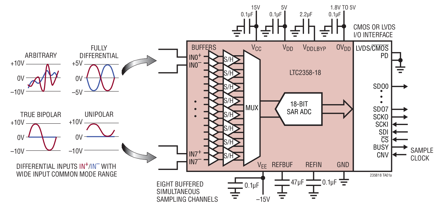
Analog Devices Inc.Demonstration circuit 2677A is a reference design for robust industrial data acquisition applications for the LTC®2358-18. The LTC2358-18 is capable of high voltage measurements with a large input common range; however, the DC2677A implements input protection that allows up to 400V of continuous input protection. Combined with gas discharge tubes, which provide protection from surges, the DC2677A is capable of surviving extreme abuse.
This reference design includes the LTC2358-18 SAR ADC, ADA4522-2 dual zero-drift operational amplifier, and an LT6658 dual-output, high current reference for sensor
excitation.
The digital interface is an HSMC (high-speed mezzanine connector), which is compatible with Altera Cyclone V SoCkit and other Altera FPGA evaluation boards that support
3.3V CMOS I/O.

LTC2662 Demo Board | 5-Channel, 16-/12-Bit, 300mA, SoftSpan Current Source DACs
Analog Devices Inc.Demonstration circuit 2692A-A features the LTC2662,
5-channel, 16-bit, 300mA, current source DACs with
10ppm/°C reference in a 5mm × 5mm QFN package.
This device features per-channel SoftSpan™ configuration
of 3.125mA to 300mA, a separate supply for each
output, and an internal switch to allow any output pin to
be connected to V−.
Pin-compatible 12-bit versions are available for lower
resolution requirements on the DC2692A-B.

LTM4623EY Demo Board | 20VIN, 3A Step-Down µModule Regulator Configured as Inverting Output. –0.9VOUT to –5.2VOUT
Analog Devices Inc.Demonstration circuit 2721A-A features the LTM4623
µModule® regulator, a tiny high performance high efficiency
step-down regulator configured as an inverting
buck-boost regulator. The DC2721A-A has an operating
input voltage range of 4V to 15V and is able to provide
an output current of up to 2A. The output voltage can be
programmed between –0.6V and –5.5V. The LTM4623 is
a complete DC/DC point of load regulator in a thermally enhanced 6.25mm × 6.25mm × 1.82mm LGA package
requiring only a few input and output capacitors. The
LTM4623 data sheet must be read in conjunction with
this demo manual for working on or modifying demo circuit
2721A-A

LTC7880 Demo Board | High Voltage Dual Step-up DC/DC Converter with Digital Power System Management
Analog Devices Inc.Demonstration circuit 2728A is a high voltage, dual output boost converter with 12V to 24V input range. The output voltage is adjustable from VIN to 48V. Each output can supply 5A maximum load current. The demo board has a LTC7880 controller, which is a 60V dual output step-up controller with digital power system management. Please see LTC7880 data sheet for more detailed information.
DC2728A powers up to default settings and produces power based on configuration resistors or its nonvolatile memory (NVM) without the need for any serial bus communication. This allows easy evaluation of the DC/DC converter. To fully explore the extensive power system management features of the part, download the GUI software LTpowerPlay® onto your PC and use ADI’s I2C/SMBus/PMBus dongle DC1613A to connect to the board. LTpowerPlay allows the user to reconfigure the part on-the-fly and store the configuration in EEPROM, view telemetry of voltage, current, temperature and fault status.

DC2732A-A
Analog Devices Inc.The LTC2949 is a high precision current, voltage, temperature,?charge and energy meter for electrical and hybrid?vehicles and other isolated current sense applications. It?infers charge and energy flowing in and out of the battery?pack by monitoring simultaneously the voltage drop over?up to two sense resistors and the battery pack voltage.Low offset ?? ADCs ensure accurate measurement of?voltage and current with insignificant power loss. Continuous?integration of current and power ensures lossless?tracking of charge and energy delivered or received by?the battery pack.The built-in serial interface can be configured to support?isolated isoSPI communication to the host or as SPI?interface.The LTC2949 features 12 internally buffered high impedance?inputs (V1 to V12) for measuring voltages from?external sensors or resistor dividers allowing to measure?temperatures, HV-Link voltages, chassis isolation and?supervise contactor states. LTC2949 has up to five programmable?digital outputs which can be set to ground,?supply or toggling at 400kHz.Programmable threshold and tracking registers reduce?digital traffic to the host.Applications Electric and Hybrid Vehicles Isolated Current Sensing Backup Battery Systems High Power Portable Equipment

LTC4249 | 65V Dual Electronic Circuit Breaker with Current Monitors
Analog Devices Inc.The DC2733 is a demonstration system for the LTC4249, 65V Dual Electronic Circuit Breaker with Current Monitors. The LTC4249 provides dual independent 1.2A, 75mΩ circuit breakers that can function independently or work together in parallel. Each circuit breaker channel has its own enable, ready, and IMON pins.
The DC2733 demo board gives access to both channels of the LTC4249, including the independent RDY and IMON outputs and the EN inputs. Resistors at the IMON pins set the circuit breaker thresholds as well as the IMON current-to-voltage gains. The IC draws power from the IN1 input.
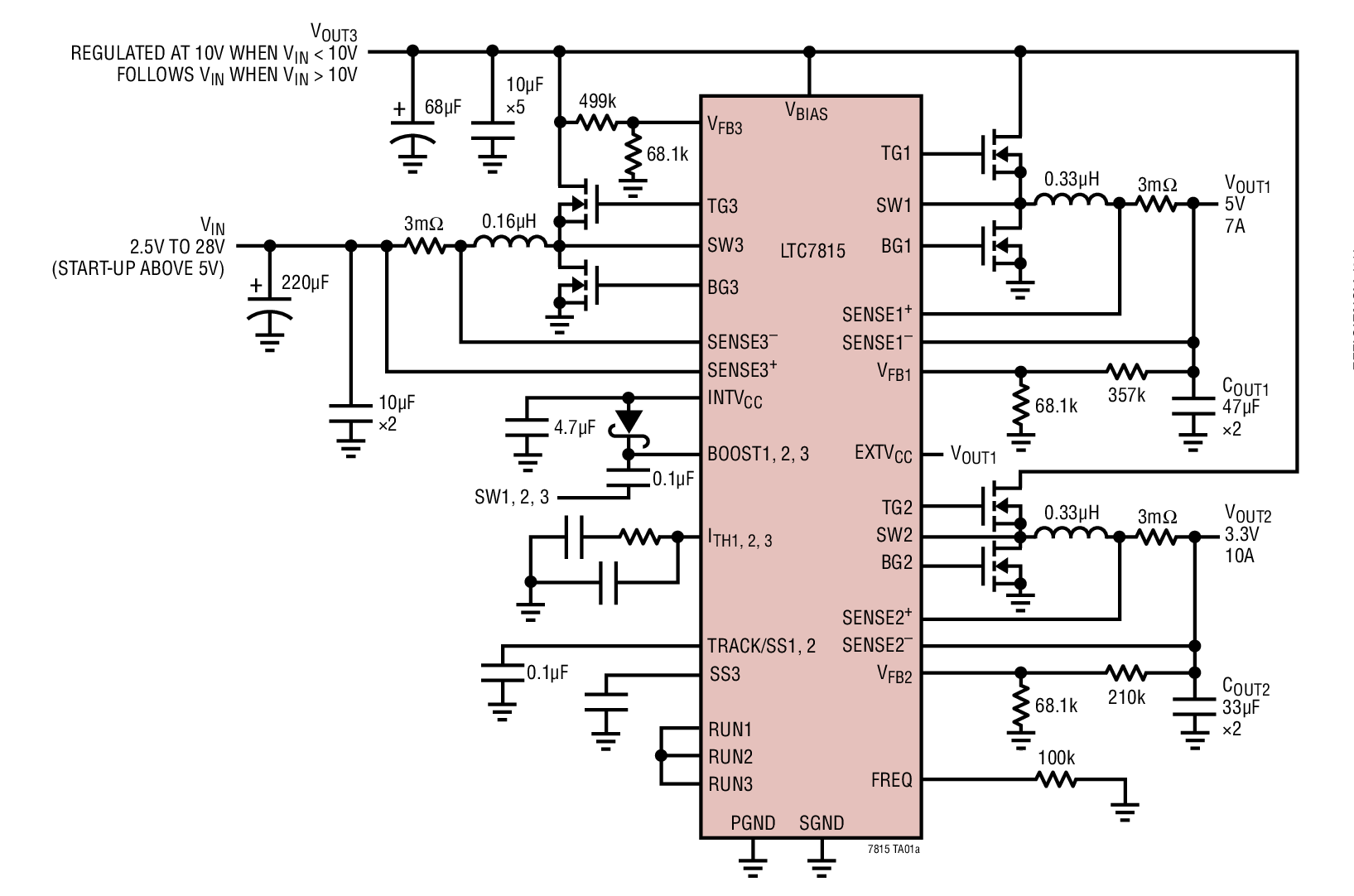
DC2738A
Analog Devices Inc.The LTC7815 is a high performance triple output (buck/buck/boost) synchronous DC/DC switching regulator controller that drives all N-channel power MOSFET stages. Constant frequency current mode architecture allows a phase-lockable switching frequency of up to 2.25MHz. The LTC7815 operates from a wide 4.5V to 38V input supply range. When biased from the output of the boost converter or another auxiliary supply, the LTC7815 can operate from an input supply as low as 2.5V after start-up.The 28?A no-load quiescent current extends operating runtime in battery powered systems. OPTI-LOOP compensation allows the transient response to be optimized over a wide range of output capacitance and ESR values. The LTC7815 features a precision 0.8V reference for the bucks, 1.2V reference for the boost and a power good output indicator. The PLLIN/MODE pin selects among Burst Mode operation, pulse-skipping mode, or continuous inductor current mode at light loads.Applications Automotive Always-On and Start-Stop Systems Battery Operated Digital Devices Distributed DC Power Systems Multioutput Buck-Boost Applications

DC273A
Analog Devices Inc.The LTC2404/LTC2408 are 4-/8-channel 2.7V to 5.5V micropower 24-bit A/D converters with an integrated oscillator, 4ppm INL and 0.3ppm RMS noise. They use delta-sigma technology and provide single cycle digital filter settling time (no latency delay) for multiplexed applications. The first conversion after the channel is changed is always valid. Through a single pin the LTC2404/LTC2408 can be configured for better than 110dB rejection at 50Hz or 60Hz ?2%, or can be driven by an external oscillator for a user defined rejection frequency in the range 1Hz to 120Hz. The internal oscillator requires no external frequency setting components. The converters accept any external reference voltage from 0.1V to VCC. With their extended input conversion range of ?12.5% VREF to 112.5% VREF the LTC2404/LTC2408 smoothly resolve the offset and overrange problems of preceding sensors or signal conditioning circuits. The LTC2404/LTC2408 communicate through a flexible 4-wire digital interface which is compatible with SPI and MICROWIRE? protocols.Applications Weight Scales Direct Temperature Measurement Gas Analyzers Strain-Gage Transducers Instrumentation Data Acquisition Industrial Process Control 6-Digit DVMs

LTM8074 1.2A Step-Down Silent Switcher µModule Regulator
Analog Devices Inc.Demonstration circuit 2753A features the LTM8074EY µModule regulator, a tiny high performance high efficiency step-down regulator with Silent Switcher® architecture. DC2753A has an operating input voltage range of 3.4V to 40V and is able to provide an output current of up to 1.2A. The output voltage can be programmed from 0.78V up to 15V. The LTM8074EY is a complete DC/DC point of load regulator in a thermally enhanced 4mm × 4mm × 1.82mm BGA package requiring only a few input and output capacitors.
The radiated EMI performances of the board (with EMI filter) are shown in Figure 6 and Figure 7. The demo board also has a conducted EMI filter installed. To use the conducted EMI filter, the input should be tied to VEMI, not VIN. An inductor L2, which is a 0Ω jumper on the board by default now, can be added in the EMI filter to further reduce the conducted emission.
The LTM8074 data sheet must be read in conjunction with this demo manual for working on or modifying DC2753A.