
LTC4223-1 | Dual Supply Hot Swap Controller for AMC (Latch Off After Fault)
Analog Devices Inc.DC1162A-A: Demo Board for LTC4223 Dual Supply Hot Swap Controller for Advanced Mezzanine Card

LT3685EMSE Demo Board | (MSOP) 6.3V ≤ VIN ≤ 38V (60V Transients), VOUT = 5V @ 2A
Analog Devices Inc.Demonstration circuit 1167 is a monolithic step-down DC/DC switching regulator featuring the LT3685 in the MSOP-10 exposed pad package. The demo board provides 5V @ 2A from a 6.3V to 38V input and has transient protection up to 60V. The demo boards default switching frequency is 500kHz, but the LT3685 has a SYNC pin which allows frequency synchronization to an external clock over a 250kHz to 2MHz range.

LTC3411AEDD Demo Board | 2.5V ≤ VIN ≤ 5.5V, VOUT = 1.8V/2.5V/3.3V @ 1.25A
Analog Devices Inc.Demonstration circuit 1176 is a step-down converter, using the LTC3411A monolithic synchronous buck regulator. The DC1176 has an input voltage range of 2.5V to 5.5V, and is capable of delivering up to 1.25A of output current. The output voltage of the DC1176 can be set to 1.8V, 2.5V or 3.3V using the appropriate jumper connection, or it can be set to an adjustable value down to 0.8V, the reference voltage of the LTC3411A.
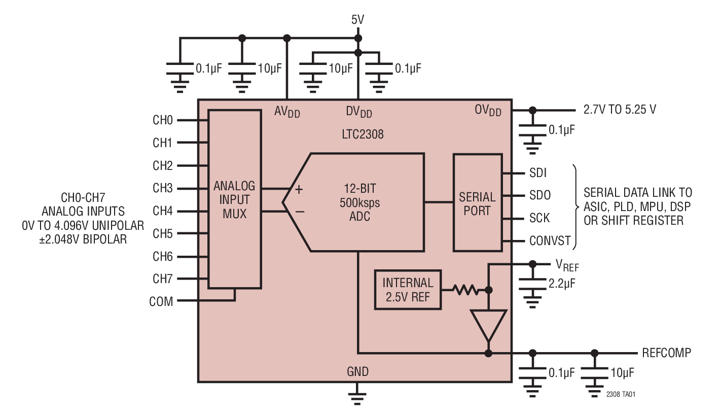
LTC2308 |12-Bit, 8-Channel SAR ADC with SPI I/F, (Requires DC590 for DC, DC890 for AC apps)
Analog Devices Inc.DC1186A: Demo Board for the LTC2308 Low Noise, 500ksps, 8-Channel, 12-Bit ADC

LTC2365 Demo Board | 12-Bit, 1Msps SAR ADC (Requires DC590B for DC Apps, DC890B for AC Apps)
Analog Devices Inc.DC1190A-B: Demo Board for the LTC2365 1Msps, 12-Bit Serial ADCs in TSOT-23

LTC2362 Demo Board | 12-Bit, 500ksps SAR ADC (Requires DC590B for DC Apps, DC890B for AC Apps)
Analog Devices Inc.DC1190A-C: Demo Board for the LTC2362 500ksps, 12-Bit Serial ADCs in TSOT-23
LTC2360 Demo Board | 12-bit, 100ksps SAR ADC (Requires DC590B for DC Apps, DC890B for AC Apps)
Analog Devices Inc.DC1190A-E: Demo Board for the LTC2360 100ksps, 12-Bit Serial ADCs in TSOT-23

LT6105 Current Sense Demo Board
Analog Devices Inc.DC1192A: Demo Board for the LT6105 Precision, Rail-to-Rail Input Current Sense Amplifier

LT3572EUF | Dual 500mA Piezo Driver & 900mA Boost Converter
Analog Devices Inc.DC1197A: Demo Board for LT3572 Dual Full-Bridge Piezo Driver with 900mA Boost Converter.

LTM4605EV Demo Board | 4.5V to 20VIN, 12VOUT @ 5A
Analog Devices Inc.Demonstration circuit DC1198B-A features the LTM4605EV, the high efficiency, high density switch mode buck-boost μModule® regulator. The LTM4605EV can regulate its output voltage from an input voltage above, below, or equal to the output. The input voltage range of DC1198B-A is from 4.5V to 20V with a preset output voltage of 12V. The rated load current is 5A, although derating is necessary for certain VIN, VOUT, and thermal conditions. The switching frequency may be synchronized to an external clock from 200kHz to 400kHz. This PLL can be used not only to reduce undesirable frequency harmonics but also to parallel LTM4605 to provide high output current.

LTM4607EV Demob Board | 6-36VIN to 12V, 5A High Efficiency Buck-Boost DC/DC µModule Regulator
Analog Devices Inc.Demonstration circuit DC1198B-B features the LTM4607EV, a high efficiency, high density switch mode buck-boost power module. The LTM4607EV can regulate its output voltage from input voltage both above and below the output. The board accepts an input voltage from 6V to 36V and is set for an output voltage of 12V. The rated load current is 5A in boost mode and 12A in step-down operation. Derating is necessary for certain VIN, VOUT and thermal conditions. The switching frequency can be synchronized to external clock operating from 200kHz to 400kHz. This clock input can be used to reduce undesirable frequency harmonics and reduce input and output ripple when paralleling LTM4607 modules for even higher output current.

LT3592EDDB Demo Board | 500mA Wide Input Voltage Range Step-Down LED Driver with 10:1 Dimming
Analog Devices Inc.DC1205A: Demo Board for LT3592 500mA Wide Input Voltage Range Step-Down LED Driver with 10:1 Dimming.

LT3504 Demo Board | Quad Buck, 5.4V ≤ VIN ≤ 40V, VOUT1 - VOUT4 = 5V/3.3V/2.5V/1.8V at 1A Each
Analog Devices Inc.The demo circuit 1207A is a quad current mode PWM stepdown DC/DC converter featuring the LT3504. The demo circuit is designed for 5V, 3.3V, 2.5V and 1.8V outputs from a 5.4V to 40V input. The current capability of each channel is up to 1A. Individual soft-start and current limit for each output as well as synchronous function simplify the complex design of quad-output power converters.
Each converter is synchronized to either a common external clock input or a resistor programmable 250kHz to 2.2MHz internal oscillator. Programmable frequency allows optimization between efficiency and external component size. Each output can be independently disabled using its own RUN/SS pin.

LTC3605EUF Demo Board | 4V ≤ VIN ≤ 15V, VOUT = 2.5V/3.3V/5V @ 5A
Analog Devices Inc.Demonstration circuit 1215 is a step-down converter, using the LTC3605 monolithic synchronous buck regulator. The DC1215A has a maximum input voltage 15V, and is capable of delivering up to 5A of output current at a minimum input voltage of 4V. The output voltage of the DC1215A can be set as low as 0.6V, the reference voltage of the LTC3605.

DC1217A
Analog Devices Inc.The LTC3230 is a low noise charge pump DC/DC converter designed to drive 4 Main LEDs and 1 Sub LED, plus two 200mA linear regulators to provide additional system power. The LTC3230 charge pump requires only four small ceramic capacitors and one current set resistor to form a complete LED power supply and current controller.Built-in soft-start circuitry prevents excessive inrush cur- rent during start-up and mode changes. High switching frequency enables the use of small external capacitors. Main and Sub full-scale current settings are programmed by a single external resistor. Charge pump efficiency is optimized based on the voltage across the LED current sources. The part powers up in 1x mode and automatically switches to the next higher mode, 1.5x and subsequently 2x, whenever any LED current source approaches dropout.Two 200mA linear regulators have independent enable and output voltage select pins. Each regulator can be set to one of three pre-selected output voltages with tri-level input pins. The regulators may be enabled independently of the charge pump.The LTC3230 is available in a low profile (0.75mm) 3mm x 3mm 20-lead QFN package.Applications Multi-LED Driver and Dual LDO Supplies for Cell Phone, PDA, Digital Camera and PND Applications?

LTC3537EUD | 600mA (I sw) Synchronous Boost Converter and 100mA LDO in 3mmmm x 3mm QFN
Analog Devices Inc.DC1242A: Demo Board for the LTC3537 - 2.2 MHz, 600mA Synchronous Step-Up DC/DC Converter and 100mA LDO

LTC3890EGN-1 Demo Board | 4.5V ≤ VIN ≤ 60V, VOUT1 = 3.3V @ 5A, VOUT2 = 8.5V @ 3A
Analog Devices Inc.Demonstration circuit 1244 is a Low Quiescent Current, Dual Output Synchronous Buck Converter featuring the LTC3890EGN-1. DC1244 converts a 4.5V to 60V voltage source to 3.3V at 5.0A and 8.5V at 3.0A. When the input voltage is close to or below 9V, the 8.5V output enters dropout mode.The "-1" version has a fixed current limit and current foldback. See data sheet for other differences.

LT3582EUD Demo Board | 2.7V-5.5VIN, Programmable Vout Boost and Inverting DC/DC Converters with OTP (Requires DC590)
Analog Devices Inc.Demonstration circuit 1247A features the LT3582 an I2C Programmable Boost and Single Inductor Inverting DC/DC Converters with OTP. It converts a 2.7V-5.5V source to two outputs, a positive and a negative. The positive output can be programmed from 3.2V to 12.775V at 25mV intervals and the negative from -1.2V to -13.95V at 50mV intervals, all via the QuickEval™ System. A DC590B is needed for evaluation of this demo board. Table 1 below shows the maximum expected load currents for some output/input combinations. Check Maximum Load Current section on datasheet for other combinations. The LT3582 features all integrated switches and feedback resistors, a low noise control scheme, positive output disconnect function, low quiescent current, built in softstart.

LTC4012CUF-2 Demo Board | Multi-Chemistry, 3A Sync Buck Battery Charger with PowerPath Control
Analog Devices Inc.Demonstration circuit DC1256A is a single-battery standalone battery charger that can support any version ofthe LTC4012 family of parts. The LTC4012 family of charge controller IC’s do not support charge termination for any specific battery chemistry. Any charger termination, if necessary, is accomplished outside the LTC4012 with the most common method using a microcontroller. The DC1256A is shipped with the LTC4012-2 installed,which is optimized for Li-ion charge applications using a 4.2V/cell float voltage.The charger output voltage is programmed by jumpers to support 1, 2, 3 and 4 series stack Li-ion batteries. The input voltage is can be between 6V and 20V with the maximum voltage of the Demo Board design limited by the input capacitor voltage ratings. To reach full charge,the minimum input voltage must be greater than the float voltage setting.

LTC6410-6 4-Port Demo Board
Analog Devices Inc.DC1264A: Demo Board for the LTC6410-6 Low Distortion, Low Noise Differential IF Amplifier with Configurable Input Impedance


