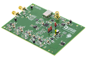
EVAL01-HMC747LC3C
Analog Devices Inc.The HMC747 is a D-Type Flip-Flop designed to support data transmission rates of up to 13 Gbps, and clock frequencies as high as 13 GHz. During normal operation, data is transferred to the outputs on the positive edge of the clock. Reversing the clock inputs allows for negative-edge triggered applications. The HMC747 also features an output level control pin, VR, which allows for loss compensation or for signal level optimization.All input and output signals to the HMC747 are terminated with 50 ? to VCC on-chip, and may be either AC or DC coupled. Inputs and outputs can be connected directly to a 50 ??to VCC terminated system, while DC blocking capacitors may be used if the terminating system is 50 ??to ground. The HMC747 operates from a single +3.3V DC supply and is available in a ceramic RoHS compliant 3?3 mm SMT package.APPLICATIONS RF ATE Applications Broadband Test & Measurement Serial Data Transmission up to 13 Gbps Digital Logic Systems up to 13 GHz
EVAL01-HMC829LP6GE
Analog Devices Inc.The HMC829LP6GE is a low noise, wide band, Fractional-N Phase-Locked-Loop (PLL) that features an integrated Voltage Controlled Oscillator (VCO ) with a fundamental frequency of 2800 MHz - 4200 MHz, and an integrated VCO Output Divider (divide by 1/2/4/6.../60/62), that together allow the HMC829LP6GE to generate frequencies from 45 MHz to 1050 MHz, from 1400 MHz to 2100 MHz, and from 2800 MHz to 4200 MHz. The integrated Phase Detector (PD) and delta-sigma modulator, capable of operating at up to 100 MHz, permit wider loop-bandwidths with excellent spectral performance.For theory of operation and register map refer to the 'PLLs w/ Integrated VCO - Microwave VCOs' Operating Guide.Applications Cellular/4G, WiMax Infrastructure Repeaters and Femtocells Communications Test Equipment CATV Equipment Phased Array Applications DDS Replacement Very High Data Rate Radios
EVAL01-HMC865LC3
Analog Devices Inc.The HMC865LC3 is a Limiting Amplifier packaged in a leadless 3x3 mm ceramic surface mount package which supports up to 43 Gbps operation. The amplifier provides 30 dB of differential gain. Output voltage swing is adjustable up to 800 mVP-P differential by using the VAC analog control input. Additive rms jitter is less than 300 fs for 32 Gbps operation. HMC865LC3 has an internal DC offset correction circuit which provides differential 10 mVP-P input sensitivity.All input/output RF signals of the HMC865LC3 are terminated with 50 Ohms to +3.3V on chip and may be either AC or DC coupled. The outputs of the device can be operated either differentially or single-ended. Outputs can be connected directly to 50 Ohm terminated system referenced to 3.3V, while DC blocking capacitors may be used if the terminating system is 50 Ohms to a non 3.3V level.APPLICATIONS 100 Gbps Ethernet 100 Gbps Long Haul 40 Gbps (D)QPSK Receivers Broadband Gain Block for?Test & Measurement Equipment
EVAL01-HMC877LC3
Analog Devices Inc.The HMC877LC3 is a phase shifter/time delay with 0 to 500?(1.4 UI) continuously adjustable shift/delay range. The delay control is linearly monotonic with respect to the differential control voltage (VDCP, VDCN) and the control input has a modulation bandwidth of 2.5 GHz. The device provides a differential output voltage with constant amplitude for single-ended or differential input voltages above the input sensitivity level, while the output voltage swing may be adjusted using the VAC control pin. The HMC877LC3 features internal temperature compensation and bias circuitry to minimize delay variations with temperature. The device also features a delay control voltage range adjustment pin, LC. All RF input and outputs of the HMC877LC3 are internally terminated with 50 Ohms to VCC, and may either be AC or DC coupled. Output pins can be connected directly to a 50 Ohm to VCC terminated system, while DC blocking capacitors must be used if the terminated system input is 50 Ohms to a DC voltage other than VCC. The HMC877LC3 is available in ROHS-compliant 3 x 3 mm SMT package.APPLICATIONS Synchronization of Clock & Data Transponder Design Broadband Test & Measurement RF ATE Applications
EVAL01-HMC954LC4B
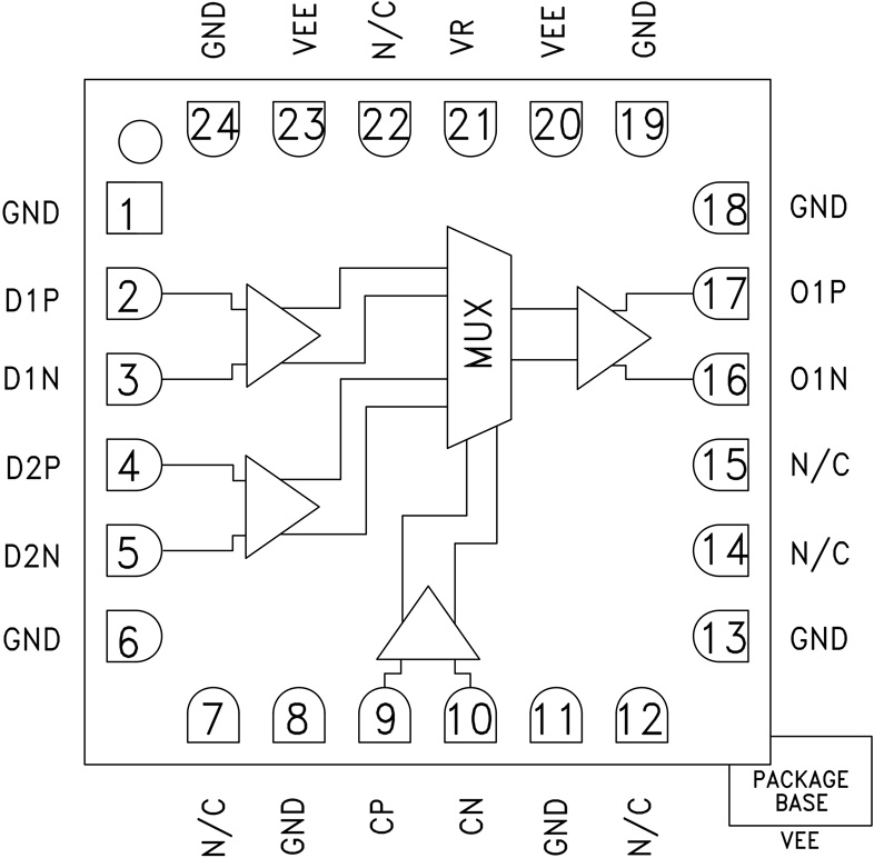
Analog Devices Inc.The HMC954LC4B is a 2 to 1 Multiplexer designed for 32 Gbps data serialization. The mux latches the two differential inputs on a rising edge of the input clock. The device uses both rising and falling edges of the half-rate clock to serialize the data. The HMC954LC4B also features an output level control pin, VR, which allows for loss compensation or for signal-level optimization.All differential inputs to the HMC954LC4B are CML and terminated on-chip with 50 ??to the positive supply, GND, and may be AC or DC coupled. The differential CML outputs are source terminated to 50 ? and may also be AC or DC coupled. Outputs can be connected directly to a 50 ??ground-terminated system or drive devices with CML logic input. The HMC954LC4B operates from a single ?3.3 V supply and is available in a ceramic ROHS-compliant 4 ? 4 mm SMT package.APPLICATIONS SONET OC-192 Broadband Test &?Measurement Equipment FPGA Interfacing Circuitry 16 G and 32 G Fiber Channel 100 Gbit Ethernet
EVAL01-HMC987LP5E
Analog Devices Inc.The HMC987LP5E 1-to-9 fanout buffer is designed for low noise clock distribution. It is intended to generate relatively square wave outputs with rise/fall times < 100 ps. The low skew and jitter outputs of the HMC987LP5E, combined with its fast rise/fall times, leads to controllable low-noise switching of downstream circuits such as mixers, ADCs/DACs or SERDES devices. The noise floor is particularly important in these applications, when the clocknetwork bandwidth is wide enough to allow squarewave switching. Driven at 2 GHz, outputs of the HMC987LP5E have a noise floor of ?166 dBc/Hz, corresponding to a jitter density of 0.6 asec/rtHz - or 50 fs over an 8 GHz bandwidth.The input stage can be driven single-ended or differentially, in a variety of signal formats (CML, LVDS, LVPECL or CMOS), AC or DC coupled. The input stage also features adjustable input impedance. It has 8 LVPECL outputs, and 1 CML output with adjustable swing/power-level in 3 dB steps.Individual output stages may be enabled or disabled for power-savings when not required using either hardware control pins, or under control of a serial-port interface.APPLICATIONS SONET, Fibre Channel,?GigE Clock Distribution ADC/DAC Clock Distribution Low Skew and Jitter Clock?or Data Fanout Wireless/Wired Communications Level Translation High Performance Instrumentation Medical Imaging Single-Ended to Differential?Conversion
EVAL-14TSSOPEBZ
Analog Devices Inc.The ADG5404 is a complementary metal-oxide semiconductor(CMOS) analog multiplexer, comprising four single channels.The on-resistance profile is very flat over the full analog input range, ensuring excellent linearity and low distortion when switching audio signals.The ADG5404 is designed on a trench process, which guardsagainst latch-up. A dielectric trench separates the P and Nchannel transistors, thereby preventing latch-up even undersevere overvoltage conditions.The ADG5404 switches one of four inputs to a common output,D, as determined by the 3-bit binary address lines, A0, A1, andEN. Logic 0 on the EN pin disables the device. Each switchconducts equally well in both directions when on and has aninput signal range that extends to the supplies. In the off condition, signal levels up to the supplies are blocked. All switchesexhibit break-before-make switching action.Product Highlights Trench Isolation Guards Against Latch-Up. A dielectric trench separates the P and N channel transistors, thereby preventing latch-up even under severe overvoltage conditions. Low RON. Dual-Supply Operation. For applications where the analog signal is bipolar, the ADG5404 can be operated from dual supplies of up to ?22 V. Single-Supply Operation. For applications where the analog signal is unipolar, the ADG5404 can be operated from a single-rail power supply of up to 40 V. 3 V logic-compatible digital inputs: VINH = 2.0 V, VINL = 0.8 V. No VL logic power supply required.Applications Relay replacement Automatic test equipment Data acquisition Instrumentation Avionics Audio and video switching Communication systems
EVAL-28TSSOPEBZ
Analog Devices Inc.The ADG5206 is a monolithic CMOS analog multiplexer comprising sixteen single channels. The ADG5206 switches one of sixteen inputs to a common output, as determined by the 4-bit binary address lines, A0, A1, A2, and A3.An EN input enables or disables the device. When EN is low, the device is disabled, and all channels switch off. The ultralow capacitance and charge injection of these switches make them ideal solutions for data acquisition and sample-and-hold applications, where low glitch and fast settling are required. Fast switching speed coupled with high signal bandwidth make these devices suitable for video signal switching.Each switch conducts equally well in both directions when on, and each switch has an input signal range that extends to the power supplies. In the off condition, signal levels up to the supplies are blocked.The ADG5206 does not have a VL pin; instead, the logic power supply is generated internally by an on-chip voltage generator.APPLICATIONS Automatic test equipment Data acquisition Instrumentation Avionics Battery Monitoring Communication systemsPRODUCT HIGHLIGHTS Trench Isolation Guards Against Latch-Up. A dielectric trench separates the P and N channel transistors to prevent latch-up even under severe overvoltage conditions. Optimal switch design for low charge injection, low switch capacitance and low leakage currents The ADG5206 achieves 8 kV HBM ESD specification on all external pins Dual-Supply Operation. For applications where the analog signal is bipolar, the ADG5206 can be operated from dual supplies of up to ?22 V. Single-Supply Operation. For applications where the analog signal is unipolar, the ADG5206 can be operated from a single rail power supply of up to 40 V.
EVAL-6SOT23EBZ
Analog Devices Inc.The ADG801 and ADG802 are monolithic CMOS, single-pole, single throw (SPST) switches with on resistance of less than 0.4 ?. These switches are designed using an advanced submicron process that provides extremely low on resistance, high switching speed, and low leakage currents.The low on resistance of
EVAL-8MSOPEBZ
Analog Devices Inc.The ADG5419 is a monolithic industrial CMOS analog switch containing a latch-up immune single-pole/double-throw (SPDT) switch. An EN input on the LFCSP package is used to enable or disable the device. When disabled, all channels are switched off.Each switch conducts equally well in both directions when on, and each switch has an input signal range that extends to the power supplies. In the off condition, signal levels up to the supplies are blocked. The ADG5419 exhibits break-before-make switching action for use in multiplexer applications.The ultralow on resistance and on-resistance flatness of these switches make them ideal solutions for data acquisition and gain switching applications, where low distortion is critical. The latch-up immune construction, and high ESD rating, makes these switches more robust in harsh environments.PRODUCT HIGHLIGHTS Trench isolation guards against latch-up. A dielectric trench separates the P and N channel transistors thereby preventing latch-up even under severe overvoltage conditions. Low RON. Dual-supply operation. For applications where the analog signal is bipolar, the ADG5419 can be operated from dual supplies up to ?22 V. Single-supply operation. For applications where the analog signal is unipolar, the ADG5419 can be operated from a single-rail power supply up to 40 V. 3 V logic compatible digital inputs: VINH = 2.0 V, VINL = 0.8 V. No VL logic power supply required.APPLICATIONS High voltage signal routing Automatic test equipment Analog front-end circuits Precision data acquisition Industrial Instrumentation Amplifier gain select Relay replacement
EVAL-AD1937AZ
Analog Devices Inc.The AD1937 is a high performance, single-chip codec that provides four analog-to-digital converters (ADCs) with differential input and eight digital-to-analog converters (DACs) with differential output, using the Analog Devices, Inc., patented multibit sigma-delta (?-?) architecture. An I2C? port is included, allowing a microcontroller to adjust volume and many other parameters. The AD1937 operates from 3.3 V digital and analog supplies. The AD1937 is available in a 64-lead (differential output) LQFP.The AD1937 is designed for low EMI. This consideration is apparent in both the system and circuit design architectures. By using the on-board PLL to derive the master clock from the LR (frame) clock or from an external crystal, the AD1937 eliminates the need for a separate high frequency master clock and can also be used with a suppressed bit clock. The DACs and ADCs are designed using the latest Analog Devices continuous time architecture to further minimize EMI. By using 3.3 V supplies, power consumption is minimized and further reduces emissions.ApplicationsAutomotive audio systems Home theater systemsSet-top boxesDigital audio effects processorsData Sheet, Rev. 0, 9/08
EVAL-AD1939AZ
Analog Devices Inc.The AD1939 is a high performance, single-chip codec that provides four analog-to-digital converters (ADCs) with differential input, and eight digital-to-analog converters (DACs) with differential output using the Analog Devices, Inc. patented multibit sigma-delta (?-?) architecture. An SPI port is included, allowing a microcontroller to adjust volume and many other parameters. The AD1939 operates from 3.3 V digital and analog supplies. The AD1939 is available in a 64-lead (differential output) LQFP package.The AD1939 is designed for low EMI. This consideration is apparent in both the system and circuit design architectures. By using the on-board PLL to derive the master clock from the LR clock or from an external crystal, the AD1939 eliminates the need for a separate high frequency master clock and can also be used with a suppressed bit clock. The DACs and ADCs are designed using the latest Analog Devices continuous time architectures to further minimize EMI. By using 3.3 V supplies, power consumption is minimized, further reducing emissions.APPLICATIONS Automotive audio systems Home Theater Systems Set-top boxes Digital audio effects processors
EVAL-AD1955EBZ
Analog Devices Inc.The AD1955 is a complete, high performance, single chip stereo digital audio playback system comprised of a multi-bit sigma-delta modulator, digital interpolation filters and a continuous-time differential current output DAC section. Unique to this audio DAC is the separate SACD (super audio CD) bit-stream and external digital filter interface, which allows users maximum system flexibility. The AD1955 supports 24-bits, 192 kHz sample rate and is designed for use in high-end SACD players, DVD-audio, home theater, automotive audio, digital mixing consoles, digital audio effect processors and sampling musical keyboards.APPLICATIONS High-End DVD-Audio, SACD, CD, Home Theatre Systems Automotive Audio Systems, Sampling Musical Keyboards, Digital Mixing Consoles, Digital Audio Effects Processors
EVAL-AD2S1205SDZ
Analog Devices Inc.The AD2S1205 is a complete 12-bit resolution tracking resolver-to-digital converter that contains an on-board programmable sinusoidal oscillator providing sine wave excitation for resolvers.The converter accepts 3.15 VP-P ? 27% input signals on the Sin and Cos inputs. A Type II tracking loop is employed to track the inputs and convert the input Sin and Cos information into a digital representation of the input angle and velocity. The maximum tracking rate is a function of the external clock frequency. The performance of the AD2S105 is specified across a frequency range of 8.192 MHz ? 25%, allowing a maximum tracking rate of 1250 rps.PRODUCT HIGHLIGHTS Ratiometric Tracking Conversion. The Type II tracking loop provides continuous output position data without conversion delay. It also provides noise immunity and tolerance of harmonic distortion on the reference and input signals. System Fault Detection. A fault detection circuit can sense loss of resolver signals, out-of-range input signals, input signal mismatch, or loss of position tracking. Input Signal Range. The Sin and Cos inputs can accept differential input voltages of 3.15 VP-P ? 27%. Programmable Excitation Frequency. Excitation frequency is easily programmable to 10 kHz, 12 kHz, 15 kHz, or 20 kHz by using the frequency select pins (the FS1 and FS2 pins). Triple Format Position Data. Absolute 12-bit angular position data is accessed via either a 12-bit parallel port or a 3-wire serial interface. Incremental encoder emulation is in standard A-quad-B format with direction output available. Digital Velocity Output. 12-bit signed digital velocity accessed via either a 12-bit parallel port or a 3-wire serial interface. APPLICATIONS Automotive motion sensing and control Hybrid-electric vehicles Electric power steering Integrated starter generator/alternator Industrial motor control Process control
EVAL-AD3552RFMC2Z
Analog Devices Inc.The AD3552R is a low drift, ultra-fast, 16-bit accuracy, current output digital-to-analog converter (DAC) that can be configured in multiple voltage span ranges. The AD3552R operates with a fixed 2.5 V reference.The device incorporates three drift compensating feedback resistors for the required external transimpedance amplifier (TIA) that scales the output voltage. Offset and gain scaling registers allow for generation of multiple output span ranges, such as 0 V to 2.5 V, 0 V to 5 V, 0 V to 10 V, ?5 V to +5 V, and ?10 V to +10 V, and custom intermediate ranges with full 16-bit resolution.The DAC can operate in fast mode for maximum speed or precision mode for maximum accuracy.The SPI interface can be configured in single SPI (classic SPI) mode, dual SPI mode, synchronous dual SPI mode, and quad SPI mode with single date rate (SDR) or double data rate (DDR), with logical levels from 1.2 V to 1.8 V.To improve device robustness, cyclic redundancy check (CRC) can be enabled. Multiple error checkers have also been integrated to detect VREF failures or memory map corruption.The AD3552R is specified over the extended industrial temperature range (?40?C to +105?C).APPLICATIONSInstrumentationHardware in the loopProcess control equipmentMedical devicesAutomatic test equipmentData acquisition systemProgrammable voltage sourcesOptical communications
EVAL-AD4002FMCZ
Analog Devices Inc.The AD4002/AD4006/AD4010 are high accuracy, high speed, low power, 18-bit, Easy Drive, precision successive approximation register (SAR) analog-to-digital converters (ADCs) that operate from a single power supply, VDD. The reference voltage, VREF, is applied externally and can be set independent of the supply voltage. The AD4002/AD4006/AD4010 power scales linearly with throughput.Easy Drive features reduce both signal chain complexity and power consumption while enabling higher channel density. The reduced input current, particularly in high-Z mode, coupled with a long signal acquisition phase, eliminates the need for a dedicated ADC driver. Easy Drive broadens the range of companion circuitry that is capable of driving these ADCs (see Figure 2 in the data sheet).Input span compression eliminates the need to provide a negative supply to the ADC driver amplifier while preserving access to the full ADC code range. The input overvoltage clamp protects the ADC inputs against overvoltage events, minimizing disturbances on the reference pin and eliminating the need for external protection diodes. Fast device throughput up to 2 MSPS allows users to accurately capture high frequency signals and to implement oversampling techniques to alleviate the challenges associated with antialias filter designs. Decreased serial peripheral interface (SPI) clock rate requirements reduce digital input/output power consumption, broadens digital host options, and simplifies the task of sending data across digital isolation. The SPI-compatible serial user interface is compatible with 1.8 V, 2.5 V, 3 V, and 5 V logic by using the separate VIO logic supply.APPLICATIONS Automated test equipment Machine automation Medical equipment Battery-powered equipment Precision data acquisition systems Instrumentation and control systems
EVAL-AD4020FMCZ
Analog Devices Inc.The AD4020 is a high accuracy, high speed, low power, 20-bit, Easy Drive, precision successive approximation register (SAR) analog-to-digital converter (ADC) that operates from a single power supply, VDD. The reference voltage, VREF, is applied externally and can be set independent of the supply voltage. The AD4020 power scales linearly with throughput.Easy Drive features reduce both signal chain complexity and power consumption while enabling higher channel density. The reduced input current, particularly in high-Z mode, coupled with a long signal acquisition phase, eliminates the need for a dedicated ADC driver. Easy Drive broadens the range of companion circuitry that is capable of driving these ADCs (see Figure 2 in the data sheet).Input span compression eliminates the need to provide a negative supply to the ADC driver amplifier while preserving access to the full ADC code range. The input overvoltage clamp protects the ADC inputs against overvoltage events, minimizing disturbances on the reference pin, and eliminating the need for external protection diodes.?Fast device throughput up to 1.8 MSPS allows users to accurately capture high frequency signals and to implement oversampling techniques to alleviate the challenges associated with antialias filter designs. Decreased serial peripheral interface (SPI) clock rate requirements reduce digital input/output power consumption, broadens digital host options, and simplifies the task of sending data across digital isolation. The SPI-compatible serial user interface is compatible with 1.8 V, 2.5 V, 3 V, and 5 V logic by using the separate VIO logic supply.APPLICATIONS Automatic test equipment Machine automation Medical equipment Battery-powered equipment Precision data acquisition systems Instrumentation and control systems
EVAL-AD4030-24-KTZ
Analog Devices Inc.The AD4030-24 is a 2 MSPS successive approximation register (SAR) analog-to-digital converter (ADC) with Easy Drive?. With a guaranteed maximum ?0.9 ppm integral nonlinearity (INL) and no missing codes at 24-bits, the AD4030-24 achieves unparalleled precision from ?40?C to +125?C. Figure 1 in the data sheet shows the functional architecture of the AD4030-24.A low-drift, internal precision reference buffer eases voltage reference sharing with other system circuitry. The AD4030-24 offers a typical dynamic range of 109 dB when using a 5 V reference. The low noise floor enables signal chains requiring less gain and lower power. A block averaging filter with programmable decimation ratio can increase dynamic range up to 155.5 dB. The wide differential input and common mode ranges allow inputs to use the full ?VREF range without saturating, simplifying signal conditioning requirements and system calibration. The improved settling of the Easy Drive analog inputs broadens the selection of analog front-end components compatible with the AD4030-24. Both single-ended and differential signals are supported.The versatile Flexi-SPI serial peripheral interface (SPI) eases host processor and ADC integration. A wide data clocking window, multiple SDO lanes, and optional DDR data clocking can reduce the serial clock to 10 MHz while operating at a sample rate of 2 MSPS. Echo clock mode and ADC host clock mode relax the timing requirements and simplify the use of digital isolators.The BGA package of the AD4030-24 integrates all critical power supply and reference bypass capacitors, reducing the footprint and system component count, and lessening sensitivity to board layout.APPLICATIONS Automatic test equipment Digital control loops Medical instrumentation Seismology Semiconductor manufacturing Scientific instrumentation
EVAL-AD4130-8WARDZ
Analog Devices Inc.The AD4130-8 is an ultra low power, high precision, measurement solution for low bandwidth battery operated applications. The fully integrated analog front end (AFE) includes a multiplexer for up to 16 single-ended or eight differential inputs, programmable gain amplifier (PGA), 24-bit sigma-delta (?-?) analog-to-digital converter (ADC), on-chip reference and oscillator, selectable filter options, smart sequencer, sensor biasing and excitation options, diagnostics, and newly added features to improve the battery-operated lifetime (more than 5 years on a coin cell), that is, a first in, first out (FIFO) buffer and duty cycling.The AD4130-8 allows users to measure low frequency signals with a current consumption of 28.5 ?A (gain = 1) and 32.5 ?A (gain = 128) while continuously converting, and even lower average currents when using one of the duty cycling options. The AD4130-8 can be configured to have 8 differential inputs or 16 single-ended or pseudo differential inputs, which connect to a crosspoint multiplexer, where any input pair can become a measurement channel input to the PGA and ADC.The AD4130-8 is designed to allow the user to operate from a single analog supply voltage from 1.71 V to 3.6 V. In battery applications, operation as low as 1.71 V can extend the system lifetime as the AFE can continue its operation, even as the battery voltage dissipates. The digital supply can be separate and range from 1.65 V to 3.6 V.Together with the reduced current consumption, the integration of an on-chip FIFO buffer can be used in tandem with the smart sequencer, to enable the AD4130-8 to become an autonomous measurement system, which allows the microcontroller to sleep for extended periods.Intelligent interrupt functionality gives the user a greater confidence in both error detection and safety. The user can enable an interrupt signal to trigger when the samples in the FIFO reach a predefined value or when a user programmable threshold is exceeded.The following key analog functions are offered on the AD4130-8 to allow simple and effective connection to transducers used for measuring temperature, load, and pressure: PGA. Due to the programmable gain (from 1 to 128) and the high input impedance with low input current, the PGA allows direct interfacing to transducers with low output amplitudes like resistive bridges, thermocouples, and resistance temperature detectors (RTDs). The capacitive PGA allows full common-mode input range, giving designers greater margin for widely varying input common modes. A wider common-mode input range improves the overall resolution and is highly effective in ratio metric measurements. Low drift precision current sources. The IEXC0 and IEXC1 current source can be used to excite 2?, 3?, and 4?wire RTDs. Excitation current output options include 100 nA, 10 ?A, 20 ?A, 50 ?A, 100 ?A, 150 ?A, and 200 ?A. The low-side power switch (PDSW) can be used to power down bridge sensors between conversions. The PDSW can be controlled within the sequencer on a per channel basis, allowing optimum timing and energy savings in the overall system. The PDSW can also allow higher powered analog sensors to be used in a low power system. Voltage bias for thermocouples (the VBIAS source sets the common-mode voltage of a channel to AVDD/2). The smart sequencer allows the conversion of each enabled preconfigured channel in a predetermined order, allowing a mix of transducer, system checks and diagnostic measurements to be interleaved. The sequencer eliminates need for repetitive serial interface communication with the device. Sixteen channels can be configured in the sequence, each of them selecting from eight predefined ADC setups that allow selection of gain, filter type, output data rate, buffering, timing, and reference source.High levels of integrated front-end functionality coupled with small package options allow smaller end solutions. For example, the AD4130-8 integrates a low thermal drift band gap reference in addition to accepting an external differential reference, which can be internally buffered.In safety critical applications the AD4130-8 includes diagnostic functionality such as open wire detection via burnout currents, internal temperature sensor, reference detection, and analog input overvoltage and undervoltage detection. Added diagnostics are included on the digital interface like cyclic redundancy check (CRC) and serial interface checks for a robust communication link.APPLICATIONS Smart transmitters Wireless battery and harvester powered sensor nodes Portable instrumentation Temperature measurement: thermocouple, RTD, thermistors Pressure measurement: bridge transducers Healthcare and wearables
EVAL-AD4630-16-KTZ
Analog Devices Inc.The AD4630-16 is a two-channel, simultaneous sampling, Easy Drive?, 2 MSPS successive approximation register (SAR) analog-to-digital converter (ADC). With a guaranteed maximum ?3 ppm integral nonlinearity (INL) and no missing codes at 16-bits, the AD4630-16 achieves excellent precision from ?40?C to +125?C. Figure 1 in the data sheet shows the functional architecture of the AD4630-16.A low-drift, internal precision reference buffer eases voltage reference sharing with other system circuitry. The AD4630-16 offers a typical dynamic range of 97.4 dB when using a 5 V reference. The low noise floor enables signal chains requiring less gain and lower power. A block averaging filter with programmable decimation ratio is available and can reduce noise for low bandwidth signals, improving accuracy. The wide differential input and common-mode ranges allow inputs to use the full (?VREF range without saturating, simplifying signal conditioning requirements and system calibration. The improved settling of the Easy Drive analog inputs broadens the selection of analog front-end components compatible with the AD4630-16. Both single-ended and differential signals are supported.The versatile Flexi-SPI serial peripheral interface (SPI) eases host processor and ADC integration. A wide data clocking window, multiple serial data output (SDO) lanes, and optional dual data rate (DDR) data clocking can reduce the serial clock to 10 MHz while operating at a sample rate of 2 MSPS. Echo clock mode can relax the timing requirements and simplify the use of digital isolators.The ball grid array (BGA) package of the AD4630-16 integrates all critical power supply and reference bypass capacitors, reducing the footprint and system component count, and lessening sensitivity to board layout.APPLICATIONS Automatic test equipment Digital control loops Medical instrumentation Seismology Semiconductor manufacturing Scientific instrumentation


