
EV-RAPID-ESL2-433Z
Analog Devices Inc.The ADuCM3027/ADuCM3029 microcontroller units (MCUs) are ultra low power microcontroller systems with integrated power management for processing, control, and connectivity. The MCU system is based on the ARM? Cortex?-M3 processor, a collection of digital peripherals, embedded SRAM and flash memory, and an analog subsystem which provides clocking, reset, and power management capability in addition to an analog-to-digital converter (ADC) subsystem. For a feature comparison across the ADuCM3027/ADuCM3029 product offerings, see Table 1. Table 1. Product Flash Memory Options Device Embedded Flash Memory Size ADuCM3029 256 kB ADuCM3027 128 kB System features that are common across the ADuCM3027/ADuCM3029/ADuCM3029-1/ADuCM3029-2 MCUs include the following: Up to 26 MHz ARM Cortex-M3 processor Up to 256 kB of embedded flash memory with error correction code (ECC) Optional 4 kB cache for lower active power 64 kB system SRAM with parity Power management unit (PMU) Multilayer advanced microcontroller bus architecture (AMBA) bus matrix Central direct memory access (DMA) controller Beeper interface Serial port (SPORT), serial peripheral interface (SPI), inter-integrated circuit (I2C), and universal asynchronous receiver/transmitter (UART) peripheral interfaces Cryptographic hardware support with advanced encryption standard (AES) and secure hash algorithm (SHA)-256 Real-time clock (RTC) General-purpose and watchdog timers Programmable general-purpose input/output (GPIO) pins Hardware cyclic redundancy check (CRC) calculator with programmable generator polynomial Power-on reset (POR) and power supply monitor (PSM) 12-bit successive approximation register (SAR) ADC True random number generator (TRNG)To support low dynamic and hibernate power management, the ADuCM3027/ADuCM3029 MCUs provide a collection of power modes and features, such as dynamic and software controlled clock gating and power gating.The ADuCM3029-1 and ADuCM3029-2 MCU models share the same features and functionality as that of the ADuCM3029 MCU. All specifications pertaining to the ADuCM3027 and ADuCM3029 are also applicable to the ADuCM3029-1 and ADuCM3029-2.For full details on the ADuCM3027/ADuCM3029 MCUs, refer to the ADuCM302x Ultra Low Power ARM Cortex-M3 MCU with Integrated Power Management Hardware Reference Manual.Product Highlights Industry leading ultralow power consumption. Robust operation, including full voltage monitoring in deep sleep modes, ECC support on flash, and parity error detection on SRAM memory. Leading edge security. Fast encryption provides read protection to customer algorithms. Write protection prevents device reprogramming by unauthorized code. Failure detection of 32 kHz LFXTAL via interrupt. SensorStrobe? for precise time synchronized sampling of external sensors. Works in hibernate mode, resulting in drastic current reduction in system solutions. Current consumption reduces by 10 times when using, for example, the ADXL363 accelerometer. Software intervention is not required after setup. No pulse drift due to software execution.Applications Internet of Things (IoT) Electronic shelf label (ESL) and signage Smart infrastructure Smart lock Asset tracking Smart machine, smart metering, smart building, smart city, and smart agriculture Wearables Fitness and clinical Machine learning and neural network?

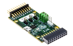
EV-RPG2-PLZ
Analog Devices Inc.The ADIN2299 is a complete, pretested solution that manages the industrial protocol and network traffic for an applications processor.The module contains everything needed to participate in a Ether-CAT, PROFINET? real-time (RT) and isochronous real time (IRT), EtherNet/IP network, including a communications controller, protocol stack, flash, RAM, follower controller, and physical layer (PHY). An applications processor connects via a universal asynchronousreceiver transmitter (UART), serial peripheral interface (SPI), or Ethernet interface.At the software layer, the applications processor connects to a unified interface so the supported industrial protocols can be used without changing the applications processor software. The ADIN2299 platform was precertified so that the field device can operate in any of the supported industrial Ethernet networks.PRODUCT HIGHLIGHTSMultiprotocol supportSmall form factor for embedded applicationsLow power and low latencyRobust network policing ensures passing PROFINET Netload Class 3APPLICATIONS Factory and process automation Motion control Building automation Transportation

GM-HX07609AA
Analog Devices Inc.SmartMesh IP wireless sensor networks are self managing, low power internet protocol (IP) networks built from wireless nodes called motes. The LTC5800-IPM is the SmartMesh IP integrated circuit in the Eterna? family of IEEE 802.15.4e System-on-Chip (SoC) solutions, featuring a highly integrated, low power radio design as well as an ARM Cortex-M3 32-bit microprocessor running SmartMesh IP embedded networking software.With SmartMesh IP time-synchronized networks, all motes in the network may route, source or terminate data, while providing many years of battery powered operation. SmartMesh IP is a highly flexible network with proven reliability and low power performance in an easy-to-integrate platform.The LTC5800-IPM?s behavior in a SmartMesh IP network is determined by the choice of SmartMesh IP network software loaded: Wireless Mote, EManager, or Access Point Mote in a SmartMesh IP network. The SmartMesh IP software provided with the LTC5800-IPM is fully tested and validated, and is readily configured via a software Application Programming Interface. Once you have purchased SmartMesh IP products, the SmartMesh IP stack binaries may be downloaded via your myAnalog account.The pin signaling behavior of the LTC5800*WR-IPMA hardware is determined by the software loaded and is described in detail in the following product datasheets: LTC5800-IPM = LTC5800*WR-IPMA hardware + SmartMesh IP ?Mote? Software ? LTC5800-IPM Datasheet LTC5800-IPR = LTC5800*WR-IPMA hardware + SmartMesh IP EManager Software ? LTC5800-IPR Datasheet LTC5800-IPA = LTC5800*WR-IPMA hardware + SmartMesh IP Access Point Software ? LTC5800-IPA Datasheet Network Features Feature Benefit >99.999% Network Reliability Avoids communications dropouts common with other wireless networks NIST-certified AES-128 bit Encryption Data protected by end-to-end encryption, message integrity checking and device authentication Scalable Uses time-slotted channel-hopping protocol to avoid in-network collisions to maximize scale while minimizing power and latency-hungry transmission retries due to congestion Bidirectional Communications Ideal for both monitoring and control applications Up to 10 messages/second/node Time-slotted communications avoids contention. This data rate includes built-in margin for packet retries. Device Features Feature Benefit Industry-Leading Low Power Radio Technology ? 4.5mA to Receive a Packet ? 5.4mA to Transmit at 0dBm ? 9.7mA to Transmit at 8dBm Pre-engineered RF RF elements include an on-chip power amplifier and are pre-tuned for optimized performance, including temperature compensation, saving development time. Energy Harvesting Support Very low power design enables motes to be powered by a wide variety of energy harvesters. Click here to see a demonstration circuit of a SmartMesh IP mote powered by indoor light. Integrated Temperature Sensor Precise temperature sensor is integrated directly into the mote. ApplicationsSmartMesh IP is ideally suited for wireless Industrial Internet of Things (IoT) applications. Learn more about SmartMesh applications.?

LT1962 Signal Chain Evaluation Board | 300mA Low Noise Positive LDO
Analog Devices Inc.Demonstration circuit SCP-LT1962-EVALZ is a 20V, 300mA Low Dropout (LDO) regulator designed to allow low noise operation in noise sensitive circuits. It is easily configured for a wide output range and can provide extremely quiet operation with its high PSRR.
Like all boards in the Signal Chain Power series, this board is designed to be easily plugged into other SCP boards to form a complete signal chain power system, enabling fast evaluation of low power signal chains. To evaluate this board, some universal SCP hardware is required, namely:
SCP-INPUT-EVALZ
SCP-OUTPUT-EVALZ
SCP-1X5BKOUT-EVALZ
SCP-THRUBRD-EVALZ
SCP-FILTER-EVALZ
SCP-1X2BKOUT-EVALZ
SCP-5X1-EVALZ
To properly evaluate SCP series demo boards, you will need the SCP Configurator companion software. SCP Configurator can help you choose the right board and topology for your design.
Note that the Demo Manual does not cover details important to the operation and configuration regarding the LT1962. Please refer to the LT1962 data sheet for a complete description of the part.

LT3045-1 Signal Chain Evaluation Board | 500mA Ultra Low Noise Positive LDO
Analog Devices Inc.Demonstration circuit SCP-LT3045-1-EVALZ is a 20V, 500mA Low Dropout (LDO) regulator designed best in class low noise operation in noise sensitive circuits. It is easily configured for a wide output range and can provide extremely quiet operation with its high PSRR.
Like all boards in the Signal Chain Power series, this board is designed to be easily plugged into other SCP boards to form a complete signal chain power system, enabling fast evaluation of low power signal chains. To evaluate this board, some universal SCP hardware is required, namely:
SCP-INPUT-EVALZ
SCP-OUTPUT-EVALZ
SCP-1X5BKOUT-EVALZ
SCP-THRUBRD-EVALZ
SCP-FILTER-EVALZ
SCP-1X2BKOUT-EVALZ
SCP-5X1-EVALZ
To properly evaluate SCP series demo boards, you will need the SCP Configurator companion software. SCP Configurator can help you choose the right board and topology for your design.
Note that the Demo Manual does not cover details important to the operation and configuration regarding the LT3045-1. Please refer to the LT3045-1 data sheet for a complete description of the part.

LT3471 Signal Chain Evaluation Board | Dual Boost/Inverting Converter
Analog Devices Inc.Demonstration circuit SCP-LT3471-EVALZ is a dual output converter featuring the LT3471EDD in boost and inverter configurations. Both converters are powered from the same 4.5V to 10V input source. The Boost converter puts out 12V at 300mA and the Inverter –12V at 200mA.
Like all boards in the Signal Chain Power series, this board is designed to be easily plugged into other SCP boards to form a complete signal chain power system, enabling fast evaluation of low power signal chains. To evaluate this board, some universal SCP hardware is required, namely:
SCP-INPUT-EVALZ
SCP-OUTPUT-EVALZ
SCP-1X5BKOUT-EVALZ
SCP-THRUBRD-EVALZ
SCP-FILTER-EVALZ
SCP-1X2BKOUT-EVALZ
SCP-5X1-EVALZ
To properly evaluate SCP series demo boards, you will need the SCP Configurator companion software. SCP Configurator can help you choose the right board and topology for your design.
Note that the Demo Manual does not cover details important to the operation and configuration regarding the LT3471. Please refer to the LT3471 data sheet for a complete description of the part.
AD-SYNCHRONA14-EBZ
Analog Devices Inc.The AD-SYNCHRONA14-EBZ is an ideal self-contained device to use in evaluation and prototyping of applications that need a highly accurate frequency and phase-controlled source clock. It is designed around the Analog Devices AD9545 and HMC7044 and greatly simplifies clock distribution and multi-channel synchronization in complex systems. It is intended to be used by trained professionals in a laboratory environment, and not intended as an end product for commercial use. It can be taken as a complete reference design and customised as required for any end customer applications. Full design details are made available free of charge.
The AD-SYNCHRONA14-EBZ comes in a 1U mechanical form factor. Using popular industry connector SMA and TwinAX interfaces most labs will already have the needed cables.
With its internal OCXO it can operate in standalone mode or be fed from a choice of external sources, such as 3 separate high speed differential clock inputs, a 10MHz reference and 1PPS. This flexibility combined with the capability to select either of the internal VCXO options of 100MHz or 122.88MHz, gives almost unlimited choice for the frequency of interest and accuracy needed for a wide variety of application areas.
MAX5391LEVMINIQU+
Analog Devices Inc.Digital Potentiometer Development Tools Eval Kit/System MAX5386M, MAX5388, MAX5391, and MAX5393 (Dual 256-Tap,Volatile, Low-Voltage Linear Taper Digital Potentiometers)
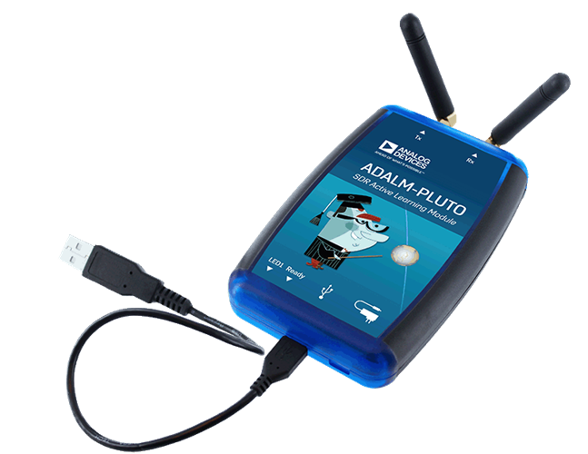
ADALM-PLUTO
Analog Devices Inc.Embark on an immersive journey into the world of RF exploration with the ADALM-PLUTO Active Learning Module, proudly presented by Analog Devices Inc. (ADI). Designed to demystify Software Defined Radio (SDR) and RF concepts, the PlutoSDR serves as a cornerstone in educational settings and beyond.
Key Highlights:
Developed by Analog Devices, a leader in semiconductor technology
Empowers students and enthusiasts to delve into RF theory and practical applications
Features the AD9363 chipset for optimal performance
Offers one receive and one transmit channel for versatile operation
Wide frequency range from 325 to 3800 MHz, coupled with up to 61.44 Mega Samples per Second (MSPS)
Compact and USB-powered for portability and convenience
Compatible with OS X™, Windows™, and Linux™ platforms for seamless integration into existing setups
Unlocking the Potential of PlutoSDR: As a testament to Analog Devices' commitment to innovation, the PlutoSDR bridges the gap between theory and practice, providing a platform for hands-on experimentation. Whether you're a student embarking on your RF journey or an experienced engineer seeking to expand your knowledge, the PlutoSDR offers a wealth of opportunities.
Seamless Integration with Leading Software: Harness the full potential of the PlutoSDR with popular software packages such as MATLAB, Simulink, and GNU Radio. Explore custom programming environments to tailor your RF experiments to your specific needs and preferences.
Empowering Education and Exploration: ADI's PlutoSDR isn't just a tool – it's a catalyst for learning and discovery. Dive into the provided documentation to unleash the full capabilities of the PlutoSDR. Engage with the vibrant community on EngineerZone to share insights, troubleshoot challenges, and collaborate on exciting projects.
Embark on Your RF Journey Today: Experience the transformative power of the ADALM-PLUTO Active Learning Module and elevate your understanding of RF systems. Whether you're a student, educator, or hobbyist, ADI's PlutoSDR is your gateway to a world of endless possibilities.
MAX5391NEVMINIQU+
Analog Devices Inc.Digital Potentiometer Development Tools Eval Kit/System MAX5386M, MAX5388, MAX5391, and MAX5393 (Dual 256-Tap,Volatile, Low-Voltage Linear Taper Digital Potentiometers)
MAX5391LEVMINIQU+
Analog Devices Inc.Digital Potentiometer Development Tools Eval Kit/System MAX5386M, MAX5388, MAX5391, and MAX5393 (Dual 256-Tap,Volatile, Low-Voltage Linear Taper Digital Potentiometers)

DC2655A-B
Analog Devices Inc.The LTC6363 family consists of four fully differential, low power, low noise amplifiers with rail-to-rail outputs optimized to drive SAR ADCs. The LTC6363 is a standalone differential amplifier, where the gain is typically set using four external resistors. The LTC6363-0.5, LTC6363-1, and LTC6363-2 each have internal matched resistors to create fixed gain blocks with gains of 0.5V/V, 1V/V, and 2V/V respectively. Each of the fixed-gain amplifiers features precision laser trimmed on-chip resistors for accurate, ultrastable gain and excellent CMRR.Applications 20-Bit, 18-Bit and 16-Bit SAR ADC Drivers Single-Ended-to-Differential Conversion Low Power ADC Drivers Level Shifter Differential Line Drivers Battery-Powered Instrumentation
DC2655A-C
Analog Devices Inc.The LTC6363 family consists of four fully differential, low power, low noise amplifiers with rail-to-rail outputs optimized to drive SAR ADCs. The LTC6363 is a standalone differential amplifier, where the gain is typically set using four external resistors. The LTC6363-0.5, LTC6363-1, and LTC6363-2 each have internal matched resistors to create fixed gain blocks with gains of 0.5V/V, 1V/V, and 2V/V respectively. Each of the fixed-gain amplifiers features precision laser trimmed on-chip resistors for accurate, ultrastable gain and excellent CMRR.Applications 20-Bit, 18-Bit and 16-Bit SAR ADC Drivers Single-Ended-to-Differential Conversion Low Power ADC Drivers Level Shifter Differential Line Drivers Battery-Powered Instrumentation

DC2663A-KIT
Analog Devices Inc.The LTC4126 is a low-power wireless single-cell Li-Ion battery charger with an integrated step-down DC/DC regulator. The step-down regulator is a low-noise multi-mode charge pump which is powered from the battery and provides a regulated 1.2V at the output. The switching frequency is set to either 50kHz or 75kHz depending on the mode to keep any switching noise out of the audible range.The LTC4126 charger is a full-featured constant-current constant-voltage Li-Ion battery charger with automatic recharge, automatic termination by safety timer, and battery temperature monitoring via an NTC pin. Charge current is fixed at 7.5mA with a 6-hour termination timer. Undervoltage protection disconnects the battery from all loads when the battery voltage is below 3.0V.The tiny 2mm ? 2mm LQFN package and minimal external component count make the LTC4126 well suited for Li-Ion battery powered hearing aid applications and other low power portable devices where a small solution size is required.Applications Hearing Aids Low Power Li-Ion Powered Devices Wireless Headsets IoT Wearables

DC2665A-A
Analog Devices Inc.The LTM4626 is a complete 12A step-down switching mode ?Module (micromodule) regulator in a tiny 6.25mm ? 6.25mm ? 3.87mm BGA package. Included in the package are the switching controller, power FETs, inductor and support components. Operating over an input voltage range of 3.1V to 20V, the LTM4626 supports an output voltage range of 0.6V to 5.5V, set by a single external resistor. Its high efficiency design delivers up to 12A continuous output current. Only bulk input and output capacitors are needed.The LTM4626 supports selectable discontinuous mode operation and output voltage tracking for supply rail sequencing. Its high switching frequency and current mode control enable a very fast transient response to line and load changes without sacrificing stability.Fault protection features include overvoltage, overcurrent and overtemperature protection.The LTM4626 is available with SnPb or RoHS compliant terminal finish.Applications Telecom, Datacom, Networking and Industrial Equipment Medical Diagnostic Equipment Data Storage Rack Units and Cards Test and Debug Systems

DC2666A-A
Analog Devices Inc.The LTC7132 is a dual output PolyPhase DC/DC synchronous step-down monolithic regulator with an I2C-based PMBus compliant serial interface. The regulator employs a constant-frequency current mode architecture, together with a unique scheme to provide excellent performance in sub-milliohm DCR applications. The LTC7132 is supported by the LTpowerPlay? software development tool with graphical user interface (GUI).Programmable loop compensation allows the regulator to be compensated digitally. The switching frequency, channel phasing and device address can be programmed both by the digital interface as well as the external configuration resistors. Additionally, parameters can be set via the digital interface and stored in EEPROM. Both outputs have independent power good indicators and FAULT function.The LTC7132 can be configured to operate in discontinuous (pulse-skipping) mode or forced continuous conduction mode. Each channel can deliver up to 25A of loadcurrent; the total current capability will depend on the APPLICATIONS total power dissipations on both channels.POWER CONVERSION Wide VIN Range: 4.5V to 20V VOUT Range: 0.5V to 3.5V (with Ultralow DCR Setting); 0.5V to 5.5V (Typical DCR Setting) Accurate PolyPhase? Current Sharing for Up to 6 Phases Available in a 140-Lead (9mm ? 11.25mm ? 2.22mm) BGA PackageAPPLICATIONS Telecom, Datacom and Storage Systems Industrial and Point-of-Load Applications


