LT4180EGN Demo Board | µ VIN = 8V to 36V, VOUT1 = 5V at 3A
Analog Devices Inc.DC1504A: Demo Board for the LT4180 Virtual Remote Sense Controller.
LT3579EFE Demo Board | 5V ≤ VIN ≤ 10V, VOUT = 12V @ 1.75A, Fault Protection
Analog Devices Inc.Demonstration circuit 1514A feature the LT3579 in A Boost Regulator configuration. The Boost is designed to convert a 5V to 10V input source to 12V at 1.75A. DC1514A is designed to survive output short circuit events with the external MOSFET installed at the input as default. The board includes an option to install the MOSFET at the output side. The LT3579 includes a 42V Master and Slave switch combination with 6A total current and can be used in many configurations such as Boost, SEPIC, Cuk and Flyback.
LT3511EMS Demo Board | 36V to 75VIN, VOUT = 5V @ 300mA
Analog Devices Inc.Demonstration circuit 1517A is a monolithic high voltage isolated flyback converter featuring the LT3511. This demo circuit is designed for a 5V isolated output from an input voltage range of 36V to 75V. The maximum output current is up to 300mA. The circuit doesn’t require an opto-isolator, due to the output voltage being sensed directly from the primary side transformer winding. A third winding off the transistor is used to bias the LT3511 for highest efficiency.
LT3956UHE Demo Board | 80VIN, 80VOUT Constant-Current, Constant-Voltage Converter
Analog Devices Inc.DC1521A: Demo Board for LT3956 80VIN, 80VOUT Constant-Current, Constant-Voltage Converter.
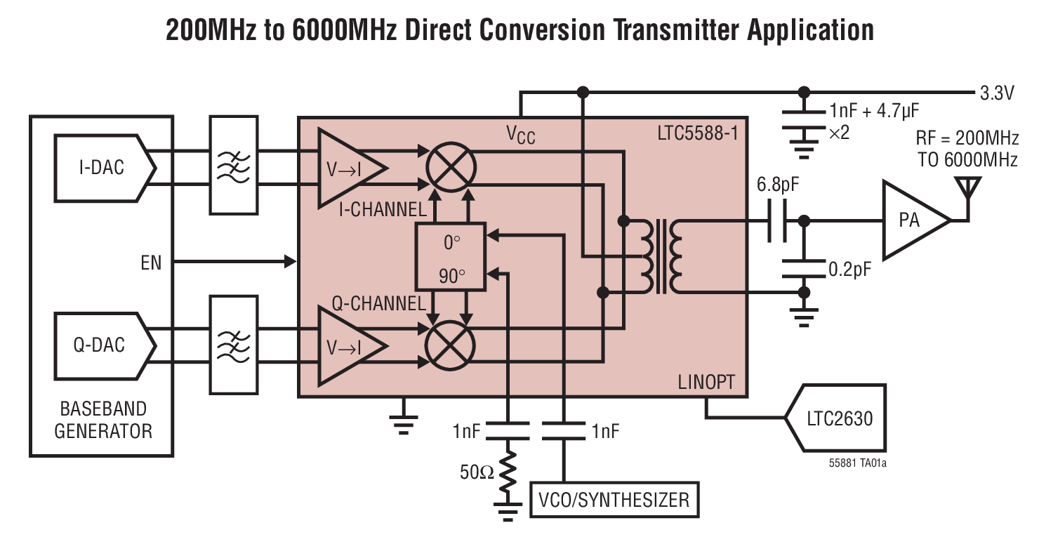
LTC5588-1 | 6GHz Ultrahigh OIP3 Quadrature Modulator
Analog Devices Inc.DC1524A-A: Demo Board for the LTC5588-1 200MHz to 6000MHz Quadrature Modulator with Ultrahigh OIP3.
DC1532A-C
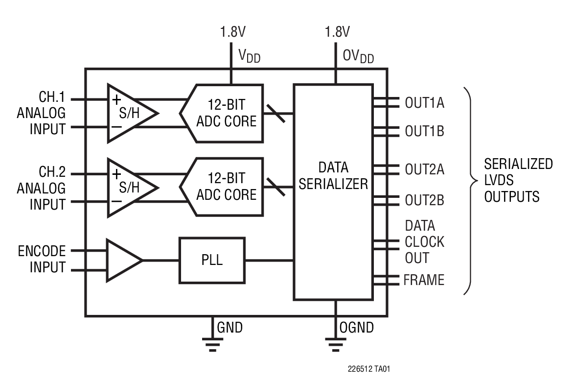
Analog Devices Inc.The LTC2268-14/LTC2267-14/LTC2266-14 are 2-channel, simultaneous sampling 14-bit A/D converters designed for digitizing high frequency, wide dynamic range signals. They are perfect for demanding communications applications with AC performance that includes 73.1dB SNR and 88dB spurious free dynamic range (SFDR). Ultralow jitter of 0.15psRMS allows undersampling of IF frequencies with excellent noise performance. DC specs include ?1LSB INL (typ), ?0.3LSB DNL (typ) and no missing codes over temperature. The transition noise is a low 1.2LSBRMS. The digital outputs are serial LVDS to minimize the number of data lines. Each channel outputs two bits at a time (2-lane mode). At lower sampling rates there is a one bit per channel option (1-lane mode). The LVDS drivers have optional internal termination and adjustable output levels to ensure clean signal integrity. The ENC+ and ENC? inputs may be driven differentially or single-ended with a sine wave, PECL, LVDS, TTL, or CMOS inputs. An internal clock duty cycle stabilizer allows high performance at full speed for a wide range of clock duty cycles. Bits LTC2266-12 12 LTC2266-14 14 Applications Communications Cellular Base Stations Software Defined Radios Portable Medical Imaging Multichannel Data Acquisition Nondestructive Testing
LTC2264-14 | 14-Bit, 40Msps, 1.8V Dual Serial ADC, 5MHz < AIN < 170MHz, Requires DC1371 and DC1075
Analog Devices Inc.DC1532A-E: Demo Board for the LTC2264-14 14-Bit, 40Msps Low Power Dual ADCs.
DC1532A-G
Analog Devices Inc.The LTC2268-12/LTC2267-12/LTC2266-12 are 2-channel, simultaneous sampling 12-bit A/D converters designed for digitizing high frequency, wide dynamic range signals. They are perfect for demanding communications applications with AC performance that includes 70.6dB SNR and 88dB spurious free dynamic range (SFDR). Ultralow jitter of 0.15psRMS allows undersampling of IF frequencies with excellent noise performance.DC specs include ?0.3LSB INL (typ), ?0.1LSB DNL (typ) and no missing codes over temperature. The transition noise is a low 0.3LSBRMS.The digital outputs are serial LVDS to minimize the number of data lines. Each channel outputs two bits at a time (2-lane mode). At lower sampling rates there is a one bit per channel option (1-lane mode). The LVDS drivers have optional internal termination and adjustable output levels to ensure clean signal integrity.The ENC+ and ENC? inputs may be driven differentially or single-ended with a sine wave, PECL, LVDS, TTL, or CMOS inputs. An internal clock duty cycle stabilizer allows high performance at full speed for a wide range of clock duty cycles. ? Bits LTC2268-12 12 LTC2268-14 14 Applications Communications Cellular Base Stations Software Defined Radios Portable Medical Imaging Multichannel Data Acquisition Nondestructive Testing
LTC2266-12 | 12-Bit, 80Msps, 1.8V Dual Serial ADC, 5MHz < AIN < 170MHz, Requires DC1371 and DC1075
Analog Devices Inc.DC1532A-I: Demo Board for the LTC2266-12 12-Bit, 80Msps Low Power Dual ADCs.
DC1532A-J
Analog Devices Inc.The LTC2265-12/LTC2264-12/LTC2263-12 are 2-channel, simultaneous sampling 12-bit A/D converters designed for digitizing high frequency, wide dynamic range signals. They are perfect for demanding communications applications with AC performance that includes 71dB SNR and 90dB spurious free dynamic range (SFDR). Ultralow jitter of 0.15psRMS allows undersampling of IF frequencies with excellent noise performance.DC specs include ?0.3LSB INL (typ), ?0.1LSB DNL (typ) and no missing codes over temperature. The transition noise is a low 0.3LSBRMS.The digital outputs are serial LVDS to minimize the number of data lines. Each channel outputs two bits at a time (2-lane mode) or one bit at a time (1-lane mode). The LVDS drivers have optional internal termination and adjustable output levels to ensure clean signal integrity.The ENC+ and ENC? inputs may be driven differentially or single-ended with a sine wave, PECL, LVDS, TTL, or CMOS inputs. An internal clock duty cycle stabilizer allows high performance at full speed for a wide range of clock duty cycles. Bits LTC2265-12 12 LTC2265-14 14 Applications Communications Cellular Base Stations Software Defined Radios Portable Medical Imaging Multichannel Data Acquisition Nondestructive Testing
LTC2264-12 | 12-Bit, 40Msps, 1.8V Dual Serial ADC, 5MHz < AIN < 170MHz, Requires DC1371 and DC1075
Analog Devices Inc.DC1532A-K: Demo Board for the LTC2264-1212-Bit, 40Msps Low Power Dual ADCs.
LT3596EUHG Demo Board | LED Driver, 6V ≤ VIN ≤ 55V, Output = 8 Series LEDs at 100mA
Analog Devices Inc.DC1542A: Demo Board for LT3596 60V Step-Down LED Driver.
DC1563A-G
Analog Devices Inc.The LTC2313-14 is a 14-bit, 2.5Msps, serial sampling A/D converter that draws only 5mA from a single 3V or 5V supply. The LTC2313-14 contains an integrated low drift reference and reference buffer providing a low cost, high performance (20ppm/?C maximum) and space saving solution. The LTC2313-14 achieves outstanding AC performance of 77dB SINAD and ?85dB THD while sampling at 2.5Msps. The extremely high sample rate-topower ratio makes the LTC2313-14 ideal for compact, low power, high speed systems. The supply current decreases at lower sampling rates as the device automatically enters nap mode after conversions.The LTC2313-14 has a high speed SPI-compatible serial interface that supports 1.8V, 2.5V, 3V and 5V logic. The fast 2.5Msps throughput with no cycle latency makes the LTC2313-14 ideally suited for a wide variety of high speed applications.? Bits LTC2313-12 12 LTC2313-14 14 Applications Communication Systems High Speed Data Acquisition Handheld Terminal Interface Medical Imaging Uninterrupted Power Supplies Battery Operated Systems Automotive
EVAL-24TSSOPEBZ
Analog Devices Inc.The ADG1414 is a monolithic complementary metal oxide semiconductor (CMOS) device containing eight independently selectable switches designed on an industrial CMOS (iCMOS?) process. iCMOS is a modular manufacturing process combining high voltage CMOS and bipolar technologies. iCMOS components can tolerate high supply voltages while providing increased performance, dramatically lower power consumption, and reduce the package size.The ADG1414 is a set of octal SPST (single-pole, single-throw) switches controlled via a 3-wire serial interface. On resistance is closely matched between switches and is very flat over the full signal range. Each switch conducts equally well in both directions and the input signal range extends to the supplies.Data is written to these devices in the form of eight bits; each bit corresponds to one channel.The ADG1414 utilizes a versatile 3-wire serial interface that operates at clock rates of up to 50 MHz and is compatible with standard SPI?, QSPI?, MICROWIRE?, and DSP interface standards. The output of the shift register, SDO, enables a number of these parts to be daisy chained.On power-up, all switches are in the off condition, and the internal registers contain all zeros.PRODUCT HIGHLIGHTS 50 MHz serial interface. 9.5 ? on resistance. 1.6 ? on-resistance flatness. 24-lead TSSOP and 4 mm ? 4 mm LFCSP packages.APPLICATIONS Automatic test equipment Data acquisition systems Battery-powered systems Sample-and-hold systems Audio signal routing Video signal routing Communication systems
EVAL-ADXL373Z
Analog Devices Inc.The ADXL373 is an ultra low power, 3-axis, ?400 g microelectromechanical systems (MEMS) accelerometer that consumes 19 ?A at a 2560 Hz output data rate (ODR). The ADXL373 does not power cycle its front end to achieve its low power operation and therefore does not run the risk of aliasing the output of the sensor.In addition to its ultra low power consumption, the ADXL373 enables impact detection while providing system level power reduction.Two additional lower power modes with interrupt driven, wake-up features are available for monitoring motion during periods of inactivity. In wake-up mode, acceleration data can be averaged to obtain a low enough output noise to trigger on low g thresholds. In instant on mode, the ADXL373 consumes 1.4 ?A while continuously monitoring the environment for impacts. When an impact event that exceeds the internally set threshold is detected, the device switches to normal operating mode fast enough to record the event.High g applications tend to experience acceleration content over a wide range of frequencies. The ADXL373 includes a four-pole, low-pass antialiasing filter to attenuate out-of-band signals that are common in high g applications. The ADXL373 also incorporates a high-pass filter to eliminate initial and slow changing errors such as ambient temperature drift.The ADXL373 provides 12-bit output data at 200 mg/LSB scale factor. The user can access configuration and data registers via the serial peripheral interface (SPI) or I2C protocol. The ADXL373 operates over a wide supply voltage range and is available in a 3.00 mm ? 3.25 mm ? 1.06 mm package.
LTC2140-14: 14-bit 25Msps Dual ADC, DDR LVDS Outputs, 5-140MHz, Requires DC890, LVDS_XFMR and DC1075
Analog Devices Inc.DC1620A-L: Demo Board for LTC2140-14 14-Bit, 25Msps Low Power Dual ADCs.
AD9653-125EBZ
Analog Devices Inc.The AD9653 is a quad, 16-bit, 125 MSPS analog-to-digital converter(ADC) with an on-chip sample-and-hold circuitdesigned for low cost, low power, small size, and ease of use.The product operates at a conversion rate of up to 125 MSPSand is optimized for outstanding dynamic performance and lowpower in applications where a small package size is critical.The ADC requires a single 1.8 V power supply and LVPECL-/CMOS-/LVDS-compatible sample rate clock for full performanceoperation. No external reference or driver components arerequired for many applications.The ADC automatically multiplies the sample rate clock for theappropriate LVDS serial data rate. A data clock output (DCO) forcapturing data on the output and a frame clock output (FCO)for signaling a new output byte are provided. Individual-channelpower-down is supported and typically consumes less than 2 mWwhen all channels are disabled. The ADC contains several featuresdesigned to maximize flexibility and minimize system cost, such as programmable output clock and data alignment and digitaltest pattern generation. The available digital test patternsinclude built-in deterministic and pseudorandom patterns, alongwith custom user-defined test patterns entered via the serial portinterface (SPI).The AD9653 is available in a RoHS-compliant, 48-lead LFCSP.It is specified over the industrial temperature range of ?40?C to+85?C.PRODUCT HIGHLIGHTS Small Footprint. Four ADCs are contained in a small, space-saving package. Low power of 163 mW/channel at 125 MSPS with scalable power options. Pin compatible to the AD9253 14-bit quad and AD9633 12-bit quad ADC. Ease of Use. A data clock output (DCO) operates at frequencies of up to 500 MHz and supports double data rate (DDR) operation. User Flexibility. The SPI control offers a wide range of flexible features to meet specific system requirementsAPPLICATIONS Medical ultrasound and MRI High speed imaging Quadrature radio receivers Diversity radio receivers Test equipment
EVAL-ADAU1860EBZ
Analog Devices Inc.The ADAU1860 is a codec with three inputs and one output that incorporates two digital signal processors (DSPs). The path from the analog input to the DSP core to the analog output is optimized for low latency and is ideal for noise canceling earphone. With the addition of just a few passive components, the ADAU1860 provides a complete earphone solution.APPLICATIONS Noise canceling handsets, headsets, and headphones Bluetooth active noise canceling (ANC) handsets, headsets, and headphones Personal navigation devices Digital still and video cameras Musical instrument effect processors Multimedia speaker systems Smartphones
EVAL-ADF7021DB9Z
Analog Devices Inc.The ADF7021 is a low power, highly integrated 2FSK/3FSK/4FSK transceiver. It is designed to operate in the narrowband, license-free ISM bands and licensed bands in the 80 MHz to 650 MHz and 862 MHz to 940 MHz frequency ranges. It has both Gaussian and raised cosine data filtering options to improve spectral efficiency for narrowband applications.It is suitable for circuit applications targeted at European ETSI-EN 300-220, the Japanese ARIB STD-T67, the Chinese Short Range Device regulations, and the North American FCC Part 15, Part 90, and Part 95 regulatory standards. A complete transceiver can be built using a small number of external discrete components, making the ADF7021 very suitable for price-sensitive and area-sensitive applications.The transmit section contains a voltage controlled oscillator (VCO) and a low noise fractional-N PLL with output resolution of
ADMV7420-EVALZ
Analog Devices Inc.The ADMV7420 is a fully integrated system in package (SiP) inphase/quadrature (I/Q) downconverter that operates betweenan intermediate frequency (IF) output range of dc and 2 GHzand a radio frequency (RF) input range of 81 GHz and 86 GHz.The device provides a small signal conversion gain of 10 dBwith 30 dBc of image rejection. The ADMV7420 uses a lownoise amplifier followed by an image rejection mixer that isdriven by a 6? local oscillator (LO) multiplier. Differential I andQ mixer outputs are provided for direct conversion applications.Alternatively, the outputs can be combined using an external90? hybrid and two external 180? hybrids for single-endedapplications.The ADMV7420 comes in a fully integrated, surface-mount,34-terminal, 11 mm ? 13 mm, chip array small outline no leadcavity (LGA_CAV) package. The ADMV7420 operates over the?40?C to +85?C case temperature range. APPLICATIONS E-band communication systems High capacity wireless backhauls Test and measurement Aerospace and defense


