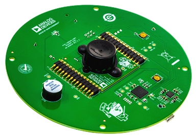
ADPD1080 Evaluation Board, optimized for motion detection and long range proximity/presence detection applications
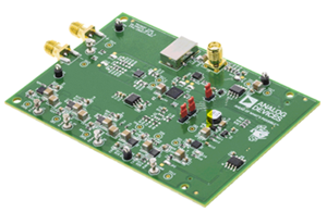
Analog Devices Inc.The EVAL-ADPD1080Z-PRX evaluation kit provides users with a simple means of connecting with the ADPD1080 hardware, collecting data from the ADPD1080, and evaluating long range proximity capabilities. The ADPD1080 hardware is configured with a large area, p-type, intrinsic, n-type (PIN) semiconductor photodiode as a proximity sensor. In this configuration, motion and proximity in front of the EVAL-ADPD1080Z-PRX are measured by detecting the amount of infrared (IR) light reflected off of objects and the change in IR light as objects move relative to the EVAL-ADPD1080Z-PRX.
The evaluation kit requires the EVAL-ADPDM3Z and the Applications Wavetool, which can be downloaded from the EVAL-ADPD1080Z-PRX product page. The Applications Wavetool is a graphical user interface (GUI) that provides users with low level and high level configurability, real-time data analysis, and user datagram protocol (UDP) transfer capabilities so that the evaluation board can easily connect to a PC.
The USB port of the PC powers the EVAL-ADPDM3Z and the EVAL-ADPD1080Z-PRX. On-board voltage regulators provide voltage supplies for the ADPD1080.
The evaluation board schematic indicates signal names for easy identification.
Full specifications for the ADPD1080 are available in the ADPD1080 data sheet. Refer to both this data sheet and the EVAL-ADPD1080Z-PRX user guide when working with the evaluation board.
EVAL-AD1940AZ
Analog Devices Inc.The AD1940 /?AD1941 are a complete 28-bit, single-chip, multi-channel audio SigmaDSP? for equalization, multiband dynamic processing, delay compensation, speaker compensation, and image enhancement. These algorithms can be used to compen-sate for the real world limitations of speakers, amplifiers, and listening environments, resulting in a dramatic improvement of perceived audio quality.The signal processing used in the AD1940 / AD1941 is comparable to that found in high end studio equipment. Most of the processing is done in full, 56-bit double-precision mode, resulting in very good, low level signal performance and the absence of limit cycles or idle tones. The dynamics processor uses a sophisticated, multiple-breakpoint algorithm often found in high end broadcast compressors. The AD1940 / AD1941 are a fully programmable DSP. Easy to use software allows the user to graphically configure a custom signal processing flow using blocks such as biquad filters, dynamics processors, and surround sound processors. An extensive control port allows click-free parameter updates, along with readback capability from any point in the algorithm flow.The AD1940 / AD1941?s digital input and output ports allow a glueless connection to ADCs and DACs by multiple, 2-channel serial data streams or TDM data streams. When in TDM mode, the AD1940 / AD1941 can input 8 or 16 channels of serial data, and can output 8 or 16 channels of serial data. The input and output port configurations can be individually set. The AD1940 is controlled by a 4-wire SPI? port; the AD1941 is controlled by a 2-wire I2C? bus. Other than the control interface, the functions of the two parts are identical. APPLICATIONS Automotive sound systems Digital televisions Home theater systems (Dolby digital/DTS postprocessor) Multichannel audio systems Mini-component stereos Multimedia audio Digital speaker crossover Musical instruments In-seat sound systems (aircrafts/motor coaches)
EVAL-AD5666SDZ
Analog Devices Inc.The AD5666 is a low power, quad, 16-bit, buffered voltage-output DAC. The part operates from a single 2.7 V to 5.5 V supply and is guaranteed monotonic by design.The AD5666 has an on-chip reference with an internal gain of 2. The AD5666-1 has a 1.25 V 5 ppm/?C reference, giving a full-scale output of 2.5 V; the AD5666-2 has a 2.5 V 5 ppm/?C reference, giving a full-scale output of 5 V. The on-board reference is off at power-up, allowing the use of an external reference. The internal reference is turned on by writing to the DAC.The part incorporates a power-on reset circuit that ensures that the DAC output powers up to 0 V (POR pin low) or to midscale (POR pin high) and remains powered up at this level until a valid write takes place. The part contains a power-down feature that reduces the current consumption of the device to 400 nA at 5 V and provides software-selectable output loads while in power-down mode for any or all DAC channels.The outputs of all DACs can be updated simultaneously using the LDAC function, with the added functionality of user-select-able DAC channels to simultaneously update. There is also an asynchronous CLR that clears all DACs to a software-selectable code?0 V, midscale, or full scale.The AD5666 utilizes a versatile 3-wire serial interface that operates at clock rates of up to 50 MHz and is compatible with standard SPI?, QSPI?, MICROWIRE?, and DSP interface standards. The on-chip precision output amplifier enables rail-to-rail output swing.Product Highlights Quad, 16-bit DAC. On-chip 1.25 V/2.5 V, 5 ppm/?C reference. Available in 14-lead TSSOP. Selectable power-on reset to 0 V or midscale. Power-down capability. When powered down, the DAC typically consumes 200 nA at 3 V and 400 nA at 5 V.Applications Process control Data acquisition systems Portable battery-powered instruments Digital gain and offset adjustment Programmable voltage and current sources Programmable attenuators
DC2769A-A-KIT
Analog Devices Inc.The LTC4124 is a simple high performance wireless Li-Ion charger with low battery disconnect. The pin-selectable charge current (up to 100mA) and charge voltage ensure versatility while minimizing the number of required external components.Wireless charging with the LTC4124 allows devices to be charged while sealed within enclosures and eliminates bulky connectors in space-constrained applications. Elimination of exposed conductive connectors also creates more robust devices while ensuring an effortless end-user experience.The LTC4124 includes an NTC input for safe temperature qualified charging and a battery disconnect feature that prevents damage to a battery due to over-discharging.The 2mm ? 2mm LQFN package and minimal number of external components make the LTC4124 well-suited for low power portable applications where small solution size is mandatory.Applications Medical Wireless Sensors Military Wearables High End Wireless Headsets Streaming Headsets with Bluetooth Connectivity Virtual Reality Headsets High End Remote Control IoT Devices
LTC4284 Demo Board | –48V, 1500W Hot Swap Controller with Telemetry and EEPROM
Analog Devices Inc.DC2909A showcases the LTC4284 high power, negative hot swap controller with telemetry and EEPROM in a –48V, 31A (1500W) application. DC2909A is configured for parallel mode, which offers reliable low cost hot plug solution for high power systems where input steps are imminent.
Included on board is isolation for power good control pins, to enable downstream power converters. LEDs indicate the presence of –48V input and output as well as the state of both supply feeds and power good signaling. High voltage layout rules are followed throughout for best long-term product reliability.
Headers are provided for three I2C interfaces, providing instant access to voltage, current, power, energy, fault log, and board temperature data.
EVAL-ADA4523-1BRMZ
Analog Devices Inc.The ADA4523-1 is a high voltage, low noise, zero drift op amp that offers precision dc performance over a wide supply range of 4.5 V to 36 V. Offset voltage and 1/f noise are suppressed, allowing this op amp to achieve a maximum offset voltage of ?4 ?V and a 0.1 Hz to 10 Hz input noise voltage of 88 nV p-p typical.The self calibrating circuitry of the ADA4523-1 results in low offset voltage drift with temperature (0.01 ?V/?C maximum) and zero drift over time. Additionally, the ADA4523-1 uses on-chip filtering to achieve high immunity to electromagnetic interference (EMI). Wide supply range, combined with low noise, low offset, 168 dB power supply rejection ratio (PSRR), and 160 dB common-mode rejection ratio (CMRR), make the ADA4523-1 well suited for high dynamic range test, measurement, and instrumentation systems.?Applications High resolution data acquisition Reference buffering Test and measurement Electronic scales Thermocouple amplifiers Strain gages Low-side current sense
LT3461 Signal Chain Evaluation Board | 1.3MHz Boost DC/DC with Int Schottky
Analog Devices Inc.Demonstration circuit SCP-LT3461-EVALZ features the LT3461 in a 12V output boost converter which operates from an input voltage of 3V to 6V. The maximum output current is 70mA when powered from a 5.0V input and 40mA when powered from a 3.3V input.
Like all boards in the Signal Chain Power series, this board is designed to be easily plugged into other SCP boards to form a complete signal chain power system, enabling fast evaluation of low power signal chains. To evaluate this board, some universal SCP hardware is required, namely:
SCP-INPUT-EVALZ
SCP-OUTPUT-EVALZ
SCP-1X5BKOUT-EVALZ
SCP-THRUBRD-EVALZ
SCP-FILTER-EVALZ
SCP-1X2BKOUT-EVALZ
SCP-5X1-EVALZ
To properly evaluate SCP series demo boards, you will need the SCP Configurator companion software. SCP Configurator can help you choose the right board and topology for your design.
Note that the Demo Manual does not cover details important to the operation and configuration regarding the LT3461. Please refer to the LT3461 data sheet for a complete description of the part.
AD9956-VCO/PCBZ
Analog Devices Inc.The AD9956 is Analog Devices?s first AgileRF synthesizer.The device is comprised of a DDS and PLL circuitry. The DDSfeatures a 14-bit DAC operating up to 400 MSPS and a 48-bitfrequency tuning word. The PLL Circuitry includes a phasedetector with scaleable 200 MHz inputs (pre-scalar inputsoperate up to 650 MHz) and digital control over the chargepump current. The device also includes a 650 MHz PECL driverwith programmable slew rates.The AD9956 uses advanced DDStechnology, an internal high-speed, high performance D/Aconverter and an advance phase-detector/charge pumpcombination to enable the synthesis of digitally-programmable,frequency-agile analog output sinusoidal waveforms up to2.7 GHz. The AD9956 is designed to provide fast frequencyhopping and fine tuning resolution (48-bit frequency tuningword). Information is loaded into the AD9956 via a serial I/Oport which has a device write speed of 25 MBit/sec. The AD9956DDS block also supports a user defined linear sweep mode ofoperation.The AD9956 is specified to operate over the extendedautomotive range of ?40?C to +125?C.Applications Agile LO frequency synthesis FM chirp source for radar and scanning systems Automotive radars Test and measurement equipment Acousto-optic device drivers
EVAL-ADG5249FEBZ
Analog Devices Inc.The ADG5248F and ADG5249F are 8:1 and dual 4:1 analog multiplexers. The ADG5248F switches one of eight inputs to a common output and the ADG5249F switches one of four differential inputs to a common differential output. Each channel conducts equally well in both directions when on, and each channel has an input signal range that extends to the supplies. The primary supply voltages define the on-resistance profile, whereas the secondary supply voltages define the voltage level at which the overvoltage protection engages.When no power supplies are present, the channel remains in the off condition, and the switch inputs are high impedance. Under normal operating conditions, if the analog input signal levels on any Sx pin exceed positive fault voltage (POSFV) or negative fault voltage (NEGFV) by a threshold voltage (VT), the channel turns off and that Sx pin becomes high impedance. If the switch is selected to be on, then the drain pin is pulled to the secondary supply voltage that was exceeded. Input signal levels up to +55 V or ?55 V relative to ground are blocked, in both the powered and unpowered condition.The low capacitance and charge injection of these switches make them ideal solutions for data acquisition and sample-and-hold applications, where low glitch switching and fast settling times are required.?Note that, throughout this data sheet, multifunction pins, such as A0/F2, are referred to either by the entire pin name or by a single function of the pin, for example, A0, when only that function is relevant.?Product Highlights Source pins are protected against voltages greater than the secondary supply rails, up to ?55 V and +55 V. Source pins are protected against voltages between ?55 V and +55 V in an unpowered state. Overvoltage detection with digital output indicates operating state of switches. Trench isolation guards against latch-up. Optimized for low charge injection and on-capacitance. The ADG5248F/ADG5249F can be operated from a dual?supply of ?5 V to ?22 V or a single power supply of 8 V to 44 V.Applications Analog input/output modules Process control/distributed control systems Data acquisition Instrumentation Avionics Automatic test equipment Communication systems Relay replacement
DC1908A-I
Analog Devices Inc.The LTC2326-16 is a low noise, high speed 16-bit successive approximation register (SAR) ADC with pseudo-differential inputs. Operating from a single 5V supply, the LTC2326-16 has a ?10.24V true bipolar input range, making it ideal for high voltage applications which require a wide dynamic range. The LTC2326-16 achieves ?1.5LSB INL maximum, no missing codes at 16 bits with 93.5dB SNR.The LTC2326-16 has an on-board single-shot capable reference buffer and low drift (20ppm/?C max) 2.048V temperature compensated reference. The LTC2326-16 also has a high speed SPI-compatible serial interface that supports 1.8V, 2.5V, 3.3V and 5V logic while also featuring a daisy-chain mode. The fast 250ksps throughput with no cycle latency makes the LTC2326-16 ideally suited for a wide variety of high speed applications. An internal oscillator sets the conversion time, easing external timing considerations. The LTC2326-16 dissipates only 28mW and automatically naps between conversions, leading to reduced power dissipation that scales with the sampling rate. A sleep mode is also provided to reduce the power consumption of the LTC2326-16 to 300?W for further power savings during inactive periods. Bits LTC2326-16 16 LTC2326-18 18 Applications Programmable Logic Controllers Industrial Process Control High Speed Data Acquisition Portable or Compact Instrumentation ATE
ADP2504CPZ-REDYKIT
Analog Devices Inc.The ADP2503?/ ADP2504 are high efficiency, low quiescent current step-up/step-down dc-to-dc converters that can operate at input voltages greater than, less than, or equal to the regulated output voltage. The power switches and synchronous rectifiers are internal to minimize external device count. At high load currents, the ADP2503 / ADP2504 use a current-mode, fixed frequency pulse-width modulation (PWM) control scheme for optimal stability and transient response. To ensure the longest battery life in portable applications, the ADP2503 / ADP2504 have an optional power save mode that reduces the switching frequency under light load conditions. For wireless and other low noise applications where variable frequency power save mode may cause interference, the logic control input sync forces fixed frequency PWM operation under all load conditions.?The ADP2503 / ADP2504 can run from input voltages between 2.3 V and 5.5 V, allowing single lithium or lithium polymer cell, multiple alkaline or NiMH cells, PCMCIA, USB, and other standard power sources. The ADP2503 / ADP2504 have fixed output options, or using the adjustable model, the output voltage can be programmed through an external resistor divider. Compensation is internal to minimize the number of external components.During logic-controlled shutdown, the input is disconnected from the output and draws less than 1 ?A from the input source. Operating as boost converters, the ADP2503 / ADP2504 feature a true load disconnect function that isolates the load from the power source. Other key features include undervoltage lockout to prevent deep battery discharge, and soft start to prevent input current overshoot at startup.APPLICATIONSWireless handsetsDigital cameras/portable audio playersMiniature hard disk power suppliesUSB powered devices?
AD8334-EVALZ
Analog Devices Inc.The AD8334 is an ultralow noise, quad channel linear-in-dB variable gain amplifier (VGA). Although optimized for ultrasound systems, it may be used as a low noise variable gain control in any application whose operating frequency is less than 100 MHz.Included in each channel are an ultralow noise preamp (LNA), an X-AMP? VGA with 48 dB of gain range, and a selectable gain postamp with adjustable output limiting. The LNA gain is 19 dB with a single-ended input and differential outputs. Using a single resistor, the LNA input impedance can be adjusted to match a signal source without compromising noise performance.The 48 dB gain range of the VGA makes these devices suitable for a variety of applications. Excellent bandwidth uniformity is maintained across the entire range. The gain control interface provides precise linear-in-dB scaling of 50 dB/V for control voltages between 40 mV and 1 V. Factory trim ensures excellent part-to-part and channel-to-channel gain matching. Differential signal paths result in superb second- and third-order distortion performance and low crosstalk.The AD8334 is a quad version of the single AD8331 and dual AD8332.For information on specs, see the AD8331/AD8332/AD8334 datasheet.Applications Ultrasound and sonar time-gain controls High performance automatic gain control (AGC) systems I/Q signal processing High speed, dual ADC drivers
123115-HMC681ALP5
Analog Devices Inc.The HMC681ALP5E is a digitally controlled variable gain amplifier which operates from DC to 1 GHz, and can be programmed to provide anywhere from 13.5 dB, to 45 dB of gain, in 0.5 dB steps. The HMC681ALP5E delivers noise figure of 2.8 dB in its maximum gain state, with output IP3 of up to +36 dBm in any state. This serially controlled digital VGA incorporates off chip AC ground capacitors for near DC operation, making it suitable for a wide variety of RF and IF applications. The HMC681ALP5E is housed in a RoHS compliant 5x5 mm QFN leadless package, and provides the user with a highly integrated solution. This functionality is also available with parallel control as the HMC626ALP5E.Applications IF & RF Applications Cellular/3G Infrastructure WiBro / WiMAX / 4G Microwave Radio & VSAT Test Equipment and Sensors
EVAL-AD7780EBZ
Analog Devices Inc.The AD7780 is a complete low power front-end solution for bridge sensor products, including weigh scales, strain gages, and pressure sensors. It contains a precision, low power, 24-bit sigma-delta (?-?) ADC; an on-chip, low noise programmable gain amplifier (PGA); and an on-chip oscillator.Consuming only 330 ?A, the AD7780 is particularly suitable for portable or battery-operated products where very low power is required. The AD7780 also has a power-down mode that allows the user to switch off the power to the bridge sensor and power down the AD7780 when not converting, thus increasing the battery life of the product.For ease of use, all the features of the AD7780 are controlled by dedicated pins. Each time a data read occurs, eight status bits are appended to the 24-bit conversion. These status bits contain a pattern sequence that can be used to confirm the validity of the serial transfer.The on-chip PGA has a gain of 1 or 128, supporting a full-scale differential input of ?5 V or ?39 mV. The device has two filter response options. The filter response at the 16.7 Hz update rate provides superior dynamic performance. The settling time is 120 ms at this update rate. At the 10 Hz update rate, the filter response provides greater than ?45 dB of stop-band attenuation. In load cell applications, this stop-band rejection is useful to reject low frequency mechanical vibrations of the load cell. The settling time is 300 ms at this update rate. Simultaneous 50 Hz/60 Hz rejection occurs at both the 10 Hz and 16.7 Hz update rates.The AD7780 operates with a power supply from 2.7 V to 5.25 V. It is available in a narrow body, 14-lead SOIC package and a 16-lead TSSOP package.ApplicationsWeigh scalesPressure MeasurementIndustrial Process ControlPortable instrumentation
LTC4359DCB Demo Board | 12V, 20A Ideal Diode with Reverse Input Protection
Analog Devices Inc.DC1502A: Demo Board for the LTC4359 Ideal Diode Controller with Reverse Input Protection.
ADRF5027-EVALZ-240
Analog Devices Inc.The ADRF5027 is a nonreflective, single-pole, double-throw (SPDT) radio frequency (RF) switch manufactured in a silicon process.The ADRF5027 operates from 9 kHz to 44 GHz with better than 3.8 dB of insertion loss and 43 dB of isolation. The ADRF5027 features an all off control, where both RF ports are in an isolation state. The ADRF5027 has a nonreflective design and both of the RF ports are internally terminated to 50 ?.The ADRF5027 requires a dual-supply voltage of +3.3 V and ?3.3 V. The device employs complimentary metal-oxide semiconductor/low-voltage transistor-transistor logic (CMOS/LVTTL) logic-compatible controls.The ADRF5027 is pin compatible with the ADRF5026 fast switching version, which operates from 100 MHz to 44 GHz.The ADRF5027 RF ports are designed to match a characteristic impedance of 50 ?. For ultrawideband products, impedance matching on the RF transmission lines can further optimize high frequency insertion loss and return loss characteristics. Refer to the Narrow-Band Impedance Matching section for an example of a matched circuit that achieves a low insertion loss response of 2.2 dB from 28 GHz to 43 GHz.The ADRF5027 comes in a 20-terminal, 3 mm ? 3 mm, RoHS-compliant, land grid array (LGA) package and can operate from ?40?C to +105?C.Applications Industrial scanners Test and instrumentation Cellular infrastructure: 5G mmWave Military radios, radars, electronic counter measures (ECMs) Microwave radios and very small aperture terminals (VSATs)
AD9744-FMC-EBZ
Analog Devices Inc.The AD97441 is a 14-bit resolution, wideband, third generation member of the TxDAC series of high performance, low power CMOS digital-to-analog converters (DACs). The TxDAC family, consisting of pin-compatible 8-, 10-, 12-, and 14-bit DACs, is specifically optimized for the transmit signal path of communication systems. All of the devices share the same interface options, small outline package, and pinout, providing an upward or downward component selection path based on performance, resolution, and cost. The AD9744 offers exceptional ac and dc performance while supporting update rates up to 210 MSPS. The AD9744?s low power dissipation makes it well suited for portable and low power applications. Its power dissipation can be further reduced to a mere 60 mW with a slight degradation in performance by lowering the full-scale current output. Also, a power-down mode reduces the standby power dissipation to approximately 15 mW. A segmented current source architecture is combined with a proprietary switching technique to reduce spurious components and enhance dynamic performance. Edge-triggered input latches and a 1.2 V temperature compensated band gap reference have been integrated to provide a complete monolithic DAC solution. The digital inputs support 3 V CMOS logic families. Product Highlights The AD9744 is the 14-bit member of the pin compatible TxDAC family, which offers excellent INL and DNL performance. Data input supports twos complement or straight binary data coding. High speed, single-ended CMOS clock input supports 210 MSPS conversion rate. Low power: Complete CMOS DAC function operates on 135 mW from a 2.7 V to 3.6 V single supply. The DAC full-scale current can be reduced for lower power operation, and a sleep mode is provided for low power idle periods. On-chip voltage reference: The AD9744 includes a 1.2 V temperature compensated band gap voltage reference. Industry-standard 28-lead SOIC, 28-lead TSSOP, and 32-lead LFCSP packages.Applications Wideband communication transmit channel Direct IFs Base stations Wireless local loops Digital radio links Direct digital synthesis (DDS) Instrumentation
DC1816B
Analog Devices Inc.The LT3799-1 is an isolated flyback controller with power factor correction specifically designed for driving LEDs. The controller operates using critical conduction mode allowing the use of a small transformer. Using a novel current sensing scheme, the controller is able to deliver a well regulated current to the secondary side without using an opto-coupler. A strong gate driver is included to drive an external high voltage MOSFET. Utilizing an onboard multiplier, the LT3799-1 typically achieves power factors of 0.97. The FAULT pin provides notification of open and short LED conditions. The LT3799-1 offers improved line regulation over the LT3799, but is not designed for use with a TRIAC dimmer.The LT3799-1 uses a micropower hysteretic start-up to efficiently operate at offline input voltages, with a third winding to provide power to the part. An internal LDO provides a well regulated supply for the part?s internal circuitry and gate driver. Triac Dimmable LED Current Regulator LT3799 Yes ? 10% LT3799-1 No ? 5% Applications Offline 4W to 100W+ LED Applications High DC VIN LED Applications
EV-TEMPSENSE-ARDZ
Analog Devices Inc.The ADT7420 is a high accuracy digital temperature sensoroffering breakthrough performance over a wide industrialrange, housed in a 4 mm ? 4 mm LFCSP package. It contains aninternal band gap reference, a temperature sensor, and a 16-bitADC to monitor and digitize the temperature to 0.0078?Cresolution. The ADC resolution, by default, is set to 13 bits(0.0625?C). The ADC resolution is a user programmable modethat can be changed through the serial interface.The ADT7420 is guaranteed to operate over supply voltages from2.7 V to 5.5 V. Operating at 3.3 V, the average supply current is typically210 ?A. The ADT7420 has a shutdown mode that powersdown the device and offers a shutdown current of typically 2.0 ?Aat 3.3 V. The ADT7420 is rated for operation over the ?40?C to+150?C temperature range.Pin A0 and Pin A1 are available for address selection, giving theADT7420 four possible I2C addresses. The CT pin is an open-drainoutput that becomes active when the temperature exceedsa programmable critical temperature limit. The INT pin is alsoan open-drain output that becomes active when the temperatureexceeds a programmable limit. The INT pin and CT pincan operate in comparator and interrupt event modes.Product Highlights Ease of use, no calibration or correction required by the user. Low power consumption. Excellent long-term stability and reliability. High accuracy for industrial, instrumentation, and medical applications. Packaged in a 16-lead, 4 mm ? 4 mm LFCSP RoHS-compliant package.Applications RTD and thermistor replacement Thermocouple cold junction compensation Medical equipment Industrial control and test Food transportation and storage Environmental monitoring and HVAC Laser diode temperature control
AD9164-FMC-EBZ
Analog Devices Inc.The AD91641 is a high performance, 16-bit digital-to-analog converter (DAC) and direct digital synthesizer (DDS) that supports update rates to 6 GSPS. The DAC core is based on a quad-switch architecture coupled with a 2? interpolator filter that enables an effective DAC update rate of up to 12 GSPS in some modes. The high dynamic range and bandwidth makes these DACs ideally suited for the most demanding high speed radio frequency (RF) DAC applications.The DDS consists of a bank of 32, 32-bit numerically controlled oscillators (NCOs), each with its own phase accumulator.When combined with a 100 MHz serial peripheral interface (SPI) and fast hop modes, phase coherent fast frequency hopping (FFH) is enabled, with several modes to support multiple applications.In baseband mode, wide analog bandwidth capability combines with high dynamic range to support DOCSIS 3.1 cable infrastructure compliance from the minimum of one carrier up to the full maximum spectrum of 1.791 GHz of signal bandwidth. A 2? interpolator filter (FIR85) enables the AD9164 to be configured for lower data rates and converter clocking to reduce the overall system power and ease the filtering requirements. In Mix-Mode? operation, the AD9164 can reconstruct RF carriers in the second and third Nyquist zones up to 7.5 GHz while still maintaining exceptional dynamic range. The output current can be programmed from 8 mA to 38.76 mA. The AD9164 data interface consists of up to eight JESD204B serializer/deserializer (SERDES) lanes that are programmable in terms of lane speed and number of lanes to enable application flexibility.An SPI interface configures the AD9164 and monitors the status of all registers. The AD9164 is offered in a 165-ball, 8 mm ? 8 mm, 0.5 mm pitch CSP_BGA package, and a 169-ball, 11 mm ? 11 mm, 0.8 mm pitch, CSP_BGA package, including a leaded ball option.Product Highlights High dynamic range and signal reconstruction bandwidth supports RF signal synthesis of up to 7.5 GHz. Up to eight lanes JESD204B SERDES interface flexible in terms of number of lanes and lane speed. Bandwidth and dynamic range to meet DOCSIS 3.1 compliance and multiband wireless communications standards with margin.?Applications Broadband communications systems DOCSIS 3.1 CMTS/ video on demand (VOD)/edge quadrature amplitude modulation (EQAM) Wireless communications infrastructure W-CDMA, LTE, LTE-A, point to point


