

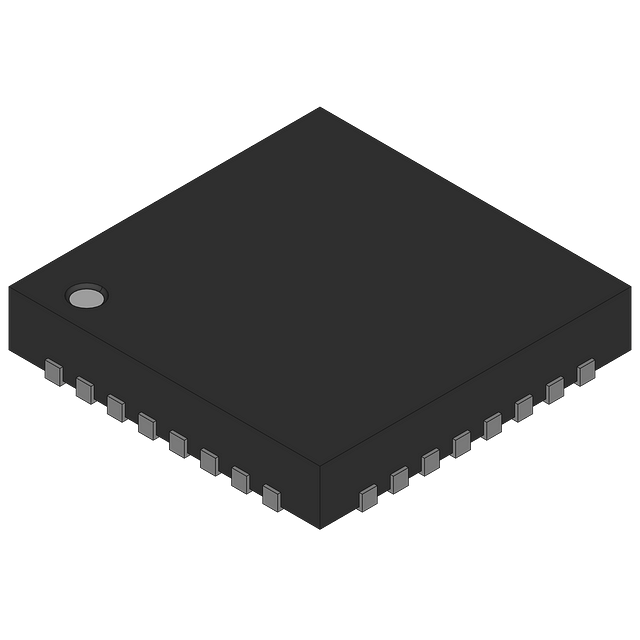
EVAL-AD7194EBZ
Analog Devices Inc.The AD7194 is a low noise, complete analog front end for high precision measurement applications. It contains a low noise, 24-bit sigma-delta (?-?) analog-to-digital converter (ADC). The on-chip low noise gain stage means that signals of small amplitude can interface directly to the ADC.The device can be configured to have eight differential inputs or sixteen pseudo differential inputs. The on-chip 4.92 MHz clock can be used as the clock source to the ADC or, alternatively, an external clock or crystal can be used. The output data rate from the part can be varied from 4.7 Hz to 4.8 kHz.The device has a very flexible digital filter, including a fast settling option. Variables such as output data rate and settling time are dependent on the option selected. For applications that require all conversions to be settled, the AD7194 includes zero latency.The part operates with a power supply from 3 V to 5.25 V. It consumes a current of 4.65 mA, and it is housed in a 32-lead LFCSP package.Applications PLC/DCS analog input modules Data acquisition Strain gage transducers Pressure measurement Temperature measurement Flow measurement Weigh scales Chromatography Medical and scientific instrumentation

EVAL-ADF4150EB1Z
Analog Devices Inc.The ADF4150 allows implementation of fractional-N or integer-N phase-locked loop (PLL) frequency synthesizers if used with an external voltage-controlled oscillator (VCO), loop filter, and external reference frequency.The ADF4150 is for use with external VCO parts and is software compatible with the ADF4350. The VCO frequency can be divided by 1/2/4/8/16 to allow the user to generate RF output frequencies as low as 31.25 MHz. For applications that require isolation the RF output stage can be muted. The mute function is both pin and software controllable.Control of all the on-chip registers is through a simple 3-wire interface. The device operates with a power supply ranging from 3.0 V to 3.6 V and can be powered down when not in use.The ADF4150 is available in a 4 mm ? 4 mm package.Applications Wireless infrastructure (W-CDMA, TD-SCDMA, WiMax, GSM, PCS, DCS, DECT) Test equipment Wireless LANs, CATV equipment Clock generation

EVAL-ADF4150HVEB1Z
Analog Devices Inc.The ADF4150HV is a 3.0 GHz, fractional-N or integer-N frequency synthesizer with an integrated high voltage charge pump. The synthesizer can be used to drive external wideband VCOs directly, eliminating the need for operational amplifiers to achieve higher tuning voltages. This simplifies design and reduces cost while improving phase noise, in contrast to active filter topologies, which tend to degrade phase noise compared to passive filter topologies.The VCO frequency can be divided by 1, 2, 4, 8, or 16 to allow the user to generate RF output frequencies as low as 31.25 MHz. For applications that require isolation, the RF output stage can be muted. The mute function is both pin- and software-controllable.A simple 3-wire interface controls all on-chip registers. The charge pump operates from a power supply ranging from 6 V to 30 V, whereas the rest of the device operates from 3.0 V to 3.6 V. The ADF4150HV can be powered down when not in use.Applications Wireless infrastructure Microwave point-to-point/point-to-multipoint radios VSAT radios Test equipment Private/land mobile radio

EVAL-ADF4151EB1Z
Analog Devices Inc.The ADF4151 allows implementation of fractional-N or integer-N phase-locked loop (PLL) frequency synthesizers if used with an external voltage controlled oscillator (VCO), loop filter, and external reference frequency.The ADF4151 is used with external VCO parts and is footprint and software compatible with the ADF4350. The part consists of a low noise digital phase frequency detector (PFD), a precision charge pump, and a programmable reference divider. There is a ?-? based fractional interpolator to allow programmable fractional-N division. The INT, FRAC, and MOD registers define an overall N divider [N = (INT + (FRAC/MOD))]. The RF output phase is programmable for applications that require a particular phase relationship between the output and the reference. The ADF4151 also features cycle slip reduction circuitry, leading to faster lock times without the need for modifications to the loop filter.Control of all the on-chip registers is through a simple 3-wire interface. The device operates with a power supply ranging from 3.0 V to 3.6 V that can be powered down when not in use.The ADF4151 is available in a 5 mm ? 5 mm package.Applications Wireless infrastructure (W-CDMA, TD-SCDMA, WiMax, GSM, PCS, DCS, DECT) Test equipment Wireless LANs, CATV equipment Clock generation
EVAL-ADF4152HVEB1Z
Analog Devices Inc.The ADF4152HV is a 5.0 GHz, fractional-N or integer N frequency synthesizer with an integrated high voltage charge pump. The synthesizer can drive external wideband voltage controlled oscillators (VCOs) directly, eliminating the need for operational amplifiers to achieve higher tuning voltages. The integrated high voltage charge pump simplifies design and reduces cost while improving phase noise, in contrast to active filter topologies, which tend to degrade phase noise compared to passive filter topologies.The VCO frequency can be divided by 1, 2, 4, 8, or 16 to allow the user to generate RF output frequencies as low as 31.25 MHz. For applications that require isolation, the RF output stage can be muted. The mute function is both pin and software controllable.A simple 3-wire interface controls all on-chip registers. The charge pump operates from a power supply ranging from 6.0 V to 30 V, whereas the rest of the device operates from 3.0 V to 3.6 V. The ADF4152HV can be powered down when not in use.Applications Wireless infrastructure Microwave point to point/point to multipoint radios Very small aperture terminal (VSAT) radios Test equipment Private land mobile radios

EVAL-ADF4154EBZ1
Analog Devices Inc.The ADF4154 is a fractional-N frequency synthesizer that implements local oscillators in the up conversion and down conversion sections of wireless receivers and transmitters. It consists of a low noise digital phase frequency detector (PFD), a precision charge pump, and a programmable reference divider. There is a ?-? based fractional interpolator to allow programmable fractional-N division. The INT, FRAC, and MOD registersdefine an overall N divider (N = (INT + (FRAC/MOD))). In addition, the 4-bit reference counter (R counter) allows selectable REFIN frequencies at the PFD input. A complete phase-locked loop (PLL) can be implemented if the synthesizer is used with an external loop filter and a voltage controlled oscillator (VCO).A key feature of the ADF4154 is the fast-lock mode with a builtintimer. The user can program a predetermined count-down time value so that the PLL will remain in wide bandwidth mode, instead of having to control this time externally.Control of all on-chip registers is via a simple 3-wire interface. The device operates with a power supply ranging from 2.7 V to 3.3 V, and can be powered down when not in use.

EVAL-ADF4350EB2Z
Analog Devices Inc.The ADF4350 allows implementation of fractional-N orinteger-N phase-locked loop (PLL) frequency synthesizersif used with an external loop filter and external referencefrequency.The ADF4350 has an integrated voltage controlled oscillator(VCO) with a fundamental output frequency ranging from2200 MHz to 4400 MHz. In addition, divide-by-1/2/4/8 or 16circuits allow the user to generate RF output frequencies as lowas 137.5 MHz. For applications that require isolation, the RFoutput stage can be muted. The mute function is both pin- andsoftware-controllable. An auxiliary RF output is also available,which can be powered down if not in use.Control of all the on-chip registers is through a simple 3-wireinterface. The device operates with a power supply rangingfrom 3.0 V to 3.6 V and can be powered down when not in use.Applications Wireless infrastructure (W-CDMA, TD-SCDMA, WiMAX, GSM, PCS, DCS, DECT) Test equipment Wireless LANs, CATV equipment Clock generation

EVAL-ADF5001EB2Z
Analog Devices Inc.The ADF5001 prescaler is a low noise, low power, fixed RF divider block that can be used to divide down frequencies as high as 18 GHz to a lower frequency suitable for input into a PLL IC, such as the?ADF4156 or ADF4106. The ADF5001 provides a divide-by-4 function. The ADF5001 operates off a 3.3 V supply and has differential 100 ? RF outputs to allow direct interface to the differential RF inputs of PLLs such as the ADF4156 and ADF4106. ApplicationsPLL frequency range extenderPoint-to-point radios VSAT radios Communications test equipment

EVAL-ADF7012DBZ4
Analog Devices Inc.The ADF7012 is a low power FSK/GFSK/OOK/GOOK/ASK UHF transmitter designed for short-range devices (SRDs). The output power, output channels, deviation frequency, and modulation type are programmable by using four, 32-bit registers.The fractional-N PLL and VCO with external inductor enable the user to select any frequency in the 75 MHz to 1 GHz band. The fast lock times of the fractional-N PLL make the ADF7012 suitable in fast frequency hopping systems. The fine frequency deviations available and PLL phase noise performance facilitates narrow-band operation.There are five selectable modulation schemes: binary frequency shift keying (FSK), Gaussian frequency shift keying (GFSK), binary on-off keying (OOK), Gaussian on-off keying (GOOK), and amplitude shift keying (ASK). In the compensation register, the output can be moved in
EVAL-ADF7012DBZ5
Analog Devices Inc.The ADF7012 is a low power FSK/GFSK/OOK/GOOK/ASK UHF transmitter designed for short-range devices (SRDs). The output power, output channels, deviation frequency, and modulation type are programmable by using four, 32-bit registers.The fractional-N PLL and VCO with external inductor enable the user to select any frequency in the 75 MHz to 1 GHz band. The fast lock times of the fractional-N PLL make the ADF7012 suitable in fast frequency hopping systems. The fine frequency deviations available and PLL phase noise performance facilitates narrow-band operation.There are five selectable modulation schemes: binary frequency shift keying (FSK), Gaussian frequency shift keying (GFSK), binary on-off keying (OOK), Gaussian on-off keying (GOOK), and amplitude shift keying (ASK). In the compensation register, the output can be moved in

EVAL-ADF7021DBZ2
Analog Devices Inc.The ADF7021 is a low power, highly integrated 2FSK/3FSK/4FSK transceiver. It is designed to operate in the narrowband, license-free ISM bands and licensed bands in the 80 MHz to 650 MHz and 862 MHz to 940 MHz frequency ranges. It has both Gaussian and raised cosine data filtering options to improve spectral efficiency for narrowband applications.It is suitable for circuit applications targeted at European ETSI-EN 300-220, the Japanese ARIB STD-T67, the Chinese Short Range Device regulations, and the North American FCC Part 15, Part 90, and Part 95 regulatory standards. A complete transceiver can be built using a small number of external discrete components, making the ADF7021 very suitable for price-sensitive and area-sensitive applications.The transmit section contains a voltage controlled oscillator (VCO) and a low noise fractional-N PLL with output resolution of
EVAL-ADF7021DBZ3
Analog Devices Inc.The ADF7021 is a low power, highly integrated 2FSK/3FSK/4FSK transceiver. It is designed to operate in the narrowband, license-free ISM bands and licensed bands in the 80 MHz to 650 MHz and 862 MHz to 940 MHz frequency ranges. It has both Gaussian and raised cosine data filtering options to improve spectral efficiency for narrowband applications.It is suitable for circuit applications targeted at European ETSI-EN 300-220, the Japanese ARIB STD-T67, the Chinese Short Range Device regulations, and the North American FCC Part 15, Part 90, and Part 95 regulatory standards. A complete transceiver can be built using a small number of external discrete components, making the ADF7021 very suitable for price-sensitive and area-sensitive applications.The transmit section contains a voltage controlled oscillator (VCO) and a low noise fractional-N PLL with output resolution of

EVAL-ADF7021-NDBZ2
Analog Devices Inc.The ADF7021-N is a high performance, low power, narrow-band transceiver based on the ADF7021. The ADF7021-N has IF filter bandwidths of 9 kHz, 13.5 kHz, and 18.5 kHz, making it ideally suited to worldwide narrowband standards and particularly those that stipulate 12.5 kHz channel separation. It is designed to operate in the narrow-band, license-free ISM bands and in the licensed bands with frequency ranges of 80 MHz to 650 MHz and 842 MHz to 916 MHz. The part has both Gaussian and raised cosine transmit data filtering options to improve spectral efficiency for narrow-band applications. It is suitable for circuit applications targeted at the Japanese ARIB STD-T67, the European ETSI EN 300 220, the Korean short range device regulations, the Chinese short range device regulations, and the North American FCC Part 15, Part 90, and Part 95 regulatory standards. A complete transceiver can be built using a small number of external discrete components, making the ADF7021-N very suitable for price-sensitive and area-sensitive applications. The range of on-chip FSK modulation and data filtering options allows users greater flexibility in their choice of modulation schemes while meeting the tight spectral efficiency requirements. The ADF7021-N also supports protocols that dynamically switch among 2FSK, 3FSK, and 4FSK to maximize communica-tion range and data throughput. The transmit section contains two voltage controlled oscillators (VCOs) and a low noise fractional-N PLL with an output resolution of The frequency-agile PLL allows the ADF7021-N to be used in frequency-hopping, spread spectrum (FHSS) systems. Both VCOs operate at twice the fundamental frequency to reduce spurious emissions and frequency pulling problems. The transmitter output power is programmable in 63 steps from ?16 dBm to +13 dBm and has an automatic power ramp control to prevent spectral splatter and help meet regulatory standards. The transceiver RF frequency, channel spacing, and modulation are programmable using a simple 3-wire interface. The device operates with a power supply range of 2.3 V to 3.6 V and can be powered down when not in use. A low IF architecture is used in the receiver (100 kHz), which minimizes power consumption and the external component count yet avoids dc offset and flicker noise at low frequencies. The IF filter has programmable bandwidths of 9 kHz, 13.5 kHz, and 18.5 kHz. The ADF7021-N supports a wide variety of pro-grammable features including Rx linearity, sensitivity, and IF bandwidth, allowing the user to trade off receiver sensitivity and selectivity against current consumption, depending on the application. The receiver also features a patent-pending automatic frequency control (AFC) loop with programmable pull-in range that allows the PLL to track out the frequency error in the incoming signal. The receiver achieves an image rejection performance of 56 dB using a patent-pending IR calibration scheme that does not require the use of an external RF source. An on-chip ADC provides readback of the integrated tempera-ture sensor, external analog input, battery voltage, and RSSI signal, which provides savings on an ADC in some applications. The temperature sensor is accurate to ?10?C over the full oper-ating temperature range of ?40?C to +85?C. This accuracy can be improved by performing a 1-point calibration at room temperature and storing the result in memory.


