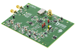
LTC4284 Demo Board | –48V, 1500W Hot Swap Controller with Telemetry and EEPROM
Analog Devices Inc.DC2909A showcases the LTC4284 high power, negative hot swap controller with telemetry and EEPROM in a –48V, 31A (1500W) application. DC2909A is configured for parallel mode, which offers reliable low cost hot plug solution for high power systems where input steps are imminent.
Included on board is isolation for power good control pins, to enable downstream power converters. LEDs indicate the presence of –48V input and output as well as the state of both supply feeds and power good signaling. High voltage layout rules are followed throughout for best long-term product reliability.
Headers are provided for three I2C interfaces, providing instant access to voltage, current, power, energy, fault log, and board temperature data.
DC782A-J
Analog Devices Inc.The LTC2228/LTC2227/LTC2226 are 12-bit 65Msps/40Msps/25Msps, low power 3V A/D converters designed for digitizing high frequency, wide dynamic range signals. The LTC2228/LTC2227/LTC2226 are perfect for demanding imaging and communications applications with AC performance that includes 71dB SNR and 80dB SFDR for signals at the Nyquist frequency.DC specs include ?0.3LSB INL (typ), ?0.15LSB DNL (typ) and no missing codes over temperature. The transition noise is a low 0.25LSBRMS.A single 3V supply allows low power operation. A separate output supply allows the outputs to drive 0.5V to 3.6V logic.A single-ended CLK input controls converter operation. An optional clock duty cycle stabilizer allows high performance at full speed for a wide range of clock duty cycles.Applications Wireless and Wired Broadband Communication Imaging Systems Ultrasound Spectral Analysis Portable Instrumentation
LTM4660 | High Density Hybrid Step-Down Synchronous Converter
Analog Devices Inc.Demonstration circuit 2879A is a high efficiency, high power density hybrid converter. It can deliver 12V/25A with an input voltage from 36V to 60V (up to 65V during transients). This demo board features the LTM4660, which uses an architecture that merges soft-switching switched capacitor topology with a traditional step-down converter to provide superior efficiency compared to the traditional switching architectures. It offers a high efficiency/high density and cost effective solution for nonisolated intermediate bus applications in power distribution, datacom and telecom.
Due to its current mode control architecture, multiple LTM4660s can be operated in a parallel, multiphase configuration with excellent current sharing and low output voltage ripple to enable much higher power applications. Other benefits include low EMI emissions due to a soft-switched front end and reduced MOSFET stress.
The LTM4660 design eliminates the inrush current typically associated with switched capacitor circuits by pre-balancing the capacitors on start-up. The LTM4660 also monitors system voltage, current and temperature for faults. It stops switching and pulls the FAULT pin low when a fault condition occurs. An onboard timer can be set for appropriate restart/retry times.
Additional features include ±1.5% output voltage accuracy over temperature, a clock output for multiphase operation, a power good output signal, short-circuit protection, monotonic output voltage start-up, optional external reference, undervoltage lockout and internal charge balance circuitry.
The LTM4660 data sheet must be used in conjunction with this demo board manual.
104991-HMC327MS8G
Analog Devices Inc.The HMC327MS8G(E) is a high efficiency GaAs InGaP Heterojunction Bipolar Transistor (HBT) MMIC Power amplifier which operates between 3 and 4 GHz. The amplifier is packaged in a low cost, surface mount 8 leaded package with an exposed base for improved RF and thermal performance. With a minimum of external components, the amplifier provides 21 dB of gain, +30 dBm of saturated power at 45% PAE from a +5V supply voltage. Power down capability is available to conserve current consumption when the amplifier is not in use.Applications Wireless Local Loop
EVAL-ADF7020DBZ3
Analog Devices Inc.The ADF7020 is a low power, low-IF transceiver designed for operation in the license-free ISM bands at 433MHz, 868MHz and 915MHz. It is suitable for circuit applications that meet either the European ETSI EN-300-220 or the North American FCC, Part 15.247 and 15.249 regulatory standards. It operates from a 2.3 V to 3.6V power supply with programmable output power from -16 to +13dBm in 0.3dBm steps. Its receiver sensitivity is -117.5dBm at 1kbits/s in FSK mode or -110.5dBm at 9.6kbits/s. Power consumption is 20mA in receive mode and 30mA in transmit mode (+10dBm output).Other features include on-chip VCO (voltage controlled oscillator), Fractional-N PLL, on-chip 7-bit ADC (analog-to-digital converter), digital received signal strength indication (RSSI), temperature sensor and a patent pending fully automatic AFC loop. This allows the ADF7020 to be used with lower tolerance crystals. Its leakage current is < 1uA in power down mode.This device is suitable for circuit applications that meet the European ETSI-300-220, the North American FCC (Part 15), or the Chinese Short Range Device regulatory standards. A complete transceiver can be built using a small number of external discrete components, making the ADF7020 very suitable for price-sensitive and area-sensitive applications. The transmitter block on the ADF7020 contains a VCO and low noise fractional-N PLL with an output resolution of
EVAL-ADUC841QSZ
Analog Devices Inc.The ADuC841/ADuC842/ADuC843 are complete smart transducer front ends, that integrates a high performance self-calibrating multichannel ADC, a dual DAC, and an optimized single-cycle 20 MHz 8-bit MCU (8051 instruction set compatible)on a single chip.The ADuC841 and ADuC842 are identical with the exception of the clock oscillator circuit; the ADuC841 is clocked directly from an external crystal up to 20 MHz whereas the ADuC842 uses a 32 kHz crystal with an on-chip PLL generating a programmable core clock up to 16.78 MHz.The ADuC843 is identical to the ADuC842 except that the ADuC843 has no analog DAC outputs.The microcontroller is an optimized 8052 core offering up to 20 MIPS peak performance. Three different memory options are available offering up to 62 kBytes of nonvolatile Flash/EE program memory. Four kBytes of nonvolatile Flash/EE data memory, 256 bytes RAM, and 2 kBytes of extended RAM are also integrated on-chip. The parts also incorporate additional analog functionality with two 12-bit DACs, power supply monitor, and a band gap reference. On-chip digital peripherals include two 16-bit ?-?. DACs, a dual output 16-bit PWM, a watchdog timer, a time interval counter, three timers/counters, and three serial I/O ports (SPI, I2C, and UART).On the ADuC812 and the ADuC832, the I2C and SPI interfaces share some of the same pins. For backwards compatibility, this is also the case for the ADuC841/ADuC842/ADuC843.However, there is also the option to allow SPI operate separately on P3.3, P3.4, and P3.5, while I2C uses the standard pins. The I2C interface has also been enhanced to offer repeated start, general call, and quad addressing.On-chip factory firmware supports in-circuit serial download and debug modes (via UART) as well as single-pin emulation mode via the EA pin..Applications Optical networking?laser power control Base station systems Precision instrumentation, smart sensors Transient capture systems DAS and communications systems
EVAL-AD5422EBZ
Analog Devices Inc.The AD5412/AD5422 are low cost, precision, fully integrated12-/16-bit digital-to-analog converters (DAC) offering a programmable current source and programmable voltage output designed to meet the requirements of industrial process control applications.The output current range is programmable at 4 mA to 20 mA, 0 mA to 20 mA, or an overrange function of 0 mA to 24 mA.The LFCSP version of this product has a CAP2 pin so that the HART signals can be coupled onto the current output of the AD5412/AD5422.Voltage output is provided from a separate pin that can be configured to provide 0 V to 5 V, 0 V to 10 V, ?5 V, or ?10 V output ranges; an overrange of 10% is available on all ranges.Analog outputs are short and open-circuit protected and can drive capacitive loads of 1 ?F.The device operates with an AVDD power supply range from 10.8 V to 40 V. Current loop compliance voltage is 0 V to AVDD ? 2.5 V.The flexible serial interface is SPI- and MICROWIRE?-compatible and can be operated in 3-wire mode to minimize the digital isolation required in isolated applications.The device also includes a power-on-reset function, ensuring that the device powers up in a known state. The part also includes an asynchronous clear pin (CLEAR) that sets the outputs to zero-scale/midscale voltage output or the low end of the selected current range.The total output error is typically ?0.01% in current mode and ?0.01% in voltage mode.Applications Process controls Actuator controls PLC HART network connectivity (LFCSP package only)
EVAL-AD4116ASDZ
Analog Devices Inc.The AD4116 is a low power, low noise, 24-bit, ?-? analog-to-digital converter (ADC) that integrates an analog front end (AFE) for six fully differential or eleven single-ended, high impedance (?10 M?) bipolar, ?10 V voltage inputs. The additional two differential or four single-ended/pseudo differential direct ADC inputs provides excellent performance at lower input ranges.The AD4116 also integrates key analog and digital signal conditioning blocks to configure eight individual setups for each analog input channel in use. As many as 16 channels can be enabled at any time. A channel is defined as any of the standard analog voltage inputs or a low level direct ADC input. The AD4116 features a maximum channel scan rate of 12,422 SPS (80 ?s) using a sinc5 + sinc1 filter and 20,618 SPS per channel (48 ?s) using a sinc3 filter.The embedded 2.5 V, low drift (5 ppm/?C), band gap internal reference (with output reference buffer) reduces the external component count.The digital filter allows flexible settings, including simultaneous 50 Hz and 60 Hz rejection at a 27.27 SPS output data rate. The user can select between the different filter settings depending on the demands of each channel in the application. The automatic channel sequencer enables the ADC to switch through each enabled channel.The precision performance of the AD4116 is achieved by integrating the proprietary iPassives? technology from Analog Devices, Inc.The AD4116 operates with a single power supply, making it easy to use in galvanically isolated applications. The specified operating temperature range is ?40?C to +105?C. The AD4116 is housed in a 40-lead, 6 mm ? 6 mm LFCSP.APPLICATIONS Process control PLC and DCS modules Instrumentation and measurement
ADMV9611-9621EVALZ-KIT
Analog Devices Inc.The ADMV9611 is a complete millimeterwave (mmWave) wireless connectivity solution in a small printed circuit assembly (PCA) format. All millimeterwave signals are confined to the printed circuit assembly, simplifying implementation. Wireless transmission is achieved using the integrated circularly polarized (CP) omnidirectional patch antenna array, which enables communication in many applications, including rotation. Following the antenna array is an integrated diplexer that provides isolation between the separate transmit and receive paths on the board, which reduces multipath distortion. The receive path integrates all components to demodulate the 58.0125 GHz frequency to baseband signals. The flexible receiver gain control is programmable over a wide range to easily accommodate the required link budget. The receiver baseband outputs are dc-coupled and can provide over 500 mV of differential output signal level. Likewise, the transmit path integrates all components to modulate input baseband signals to 63 GHz. The transmitter has programmable gain control to maintain level transmit power. The transmit baseband inputs are dc-coupled and have a broad common-mode input range. Synthesizers are integrated to maintain excellent frequency stability vs. temperature. The simple amplitude modulation (AM) scheme eliminates the need for external data converters, allowing for bit rates of greater than 100 Mbps. On-board power management is integrated to a single 5 V voltage rail to power the ADMV9611.Together with the ADMV9621, the ADMV9611 provides a complete, full duplexed 60 GHz data link for high speed data transmission in the unlicensed 60 GHz industrial, scientific, and medical (ISM) band.APPLICATIONS60 GHz short data link for industrial and medical high data rate applicationsHigh speed data for rotating applications, such as slip rings and magnetic resonance imaging systems
ADP1031CP-2-EVALZ
Analog Devices Inc.The ADP1031 is a high performance, isolated micropowermanagement unit (PMU) that combines an isolated flybackdc-to-dc regulator, an inverting dc-to-dc regulator, and abuck dc-to-dc regulator, providing three isolated power rails.Additionally, the ADP1031 contains four, high speed, serialperipheral interface (SPI) isolation channels and three general-purpose isolators for channel to channel applications where lowpower dissipation and small solution size is required.Operating over an input voltage range of +4.5 V to +60 V, theADP1031 generates isolated output voltages of +6 V to +28 V(adjustable version) or+ 21 V and +24 V (fixed versions) forVOUT1, factory programmable voltages of +5.15 V, +5.0 V, or+3.3 V for VOUT2, and an adjustable output voltages of ?24 V to?5 V for VOUT3.By default, the ADP1031 flyback regulator operates at a 250 kHzswitching frequency and the buck and inverting regulators operateat 125 kHz. All three regulators are phase shifted relative to eachother to reduce electromagnetic interference (EMI). The ADP1031can be driven by an external oscillator in the range of 350 kHzto 750 kHz to ease noise filtering in sensitive applications.The digital isolators integrated in the ADP1031 use AnalogDevices, Inc., iCoupler? chip scale transformer technology,optimized for low power and low radiated emissions.The ADP1031 is available in a 9 mm ? 7 mm, 41-lead LFCSP andis rated for a ?40?C to +125?C operating junction temperaturerange.Applications Industrial automation and process control Instrumentation and data acquisition systems Data and power isolation
ADP1031CP-3-EVALZ
Analog Devices Inc.The ADP1031 is a high performance, isolated micropowermanagement unit (PMU) that combines an isolated flybackdc-to-dc regulator, an inverting dc-to-dc regulator, and abuck dc-to-dc regulator, providing three isolated power rails.Additionally, the ADP1031 contains four, high speed, serialperipheral interface (SPI) isolation channels and three general-purpose isolators for channel to channel applications where lowpower dissipation and small solution size is required.Operating over an input voltage range of +4.5 V to +60 V, theADP1031 generates isolated output voltages of +6 V to +28 V(adjustable version) or+ 21 V and +24 V (fixed versions) forVOUT1, factory programmable voltages of +5.15 V, +5.0 V, or+3.3 V for VOUT2, and an adjustable output voltages of ?24 V to?5 V for VOUT3.By default, the ADP1031 flyback regulator operates at a 250 kHzswitching frequency and the buck and inverting regulators operateat 125 kHz. All three regulators are phase shifted relative to eachother to reduce electromagnetic interference (EMI). The ADP1031can be driven by an external oscillator in the range of 350 kHzto 750 kHz to ease noise filtering in sensitive applications.The digital isolators integrated in the ADP1031 use AnalogDevices, Inc., iCoupler? chip scale transformer technology,optimized for low power and low radiated emissions.The ADP1031 is available in a 9 mm ? 7 mm, 41-lead LFCSP andis rated for a ?40?C to +125?C operating junction temperaturerange.Applications Industrial automation and process control Instrumentation and data acquisition systems Data and power isolation
ADP1032CP-2-EVALZ
Analog Devices Inc.The ADP1032 is a high performance, isolated micropower management unit (PMU) that combines an isolated flyback and a dc-to-dc regulator providing two isolated power rails. Additionally, the ADP1032 contains four high speed serial peripheral interface (SPI) isolation channels and three general-purpose isolators for channel to channel applications where low power dissipation and small solution size is required. Operating over an input voltage range of 4.5 V to 60 V, the ADP1032 generates isolated output voltages of 6 V to 28 V (adjustable version) or 24 V (fixed version) for VOUT1, and factory programmable voltages of 5.15 V, 5.0 V, or 3.3 V for VOUT2.?By default, the ADP1032 flyback regulator operates at a 250 kHz switching frequency, and the buck regulator operates at 125 kHz.?The two regulators are phase shifted relative to each other to reduce electromagnetic interference (EMI). The ADP1032 can be driven by an external oscillator in the range of 350 kHz to 750 kHz to ease noise filtering in sensitive applications.?The digital isolators integrated in the ADP1032 use Analog Devices, Inc., iCoupler? chip scale transformer technology, optimized for low power and low radiated emissions. The ADP1032 is available in a 9 mm ? 7 mm, 41-lead LFCSP and is rated for a ?40?C to +125?C operating junction temperature range.?
ADP1032CP-5-EVALZ
Analog Devices Inc.The ADP1032 is a high performance, isolated micropower management unit (PMU) that combines an isolated flyback and a dc-to-dc regulator providing two isolated power rails. Additionally, the ADP1032 contains four high speed serial peripheral interface (SPI) isolation channels and three general-purpose isolators for channel to channel applications where low power dissipation and small solution size is required. Operating over an input voltage range of 4.5 V to 60 V, the ADP1032 generates isolated output voltages of 6 V to 28 V (adjustable version) or 24 V (fixed version) for VOUT1, and factory programmable voltages of 5.15 V, 5.0 V, or 3.3 V for VOUT2.?By default, the ADP1032 flyback regulator operates at a 250 kHz switching frequency, and the buck regulator operates at 125 kHz.?The two regulators are phase shifted relative to each other to reduce electromagnetic interference (EMI). The ADP1032 can be driven by an external oscillator in the range of 350 kHz to 750 kHz to ease noise filtering in sensitive applications.?The digital isolators integrated in the ADP1032 use Analog Devices, Inc., iCoupler? chip scale transformer technology, optimized for low power and low radiated emissions. The ADP1032 is available in a 9 mm ? 7 mm, 41-lead LFCSP and is rated for a ?40?C to +125?C operating junction temperature range.?
ADP1050DC1-EVALZ
Analog Devices Inc.The ADP1050 is an advanced digital controller with a PMBus? interface targeting high density, high efficiency dc-to-dc power conversion. This controller implements voltage mode control with high speed, input voltage feedforward operation for enhanced transient and noise performance. The ADP1050 has four programmable pulse-width modulation (PWM) outputs capable of controlling most high efficiency power supply topologies, with the added control of synchronous rectification (SR).The ADP1050 implements several features to enable a robust system of parallel and redundant operation for customers who require high availability. The device provides synchronization, prebias startup, and conditional overvoltage techniques to identify and safely shut down an erroneous power supply in parallel operation mode.The ADP1050 is based on flexible state machine architecture and is programmed using an intuitive graphical user interface (GUI). The easy to use GUI reduces design cycle time and results in a robust, hardware coded system loaded into the built-in EEPROM. The small size (4 mm ? 4 mm) of the LFCSP package makes the ADP1050 ideal for ultracompact, isolated dc-to-dc power module or embedded power designs.Applications High density, isolated dc-to-dc power supplies Intermediate bus converters High availability parallel power systems Server, storage, industrial, networking, and communications infrastructure
ADP1051DC1-EVALZ
Analog Devices Inc.The ADP1051 is an advanced digital controller with a PMBus? interface targeting high density, high efficiency dc-to-dc power conversion. This controller implements voltage mode control with high speed, input line feedforward for enhanced transient and improved noise performance. The ADP1051 has six programmable pulse-width modulation (PWM) outputs capable of controlling most high efficiency power supply topologies, with added control of synchronous rectification (SR). The device includes adaptive dead time compensation to improve efficiency over the load range, and programmable light load mode operation, combined with low power consumption, to reduce system standby power losses.The ADP1051 implements several features to enable a robust system of parallel and redundant operation for customers that require high availability or parallel connection. The device provides synchronization, reverse current protection, pre-bias startup, accurate current sharing between power supplies, and conditional overvoltage techniques to identify and safely shut down an erroneous power supply in parallel operation mode.The ADP1051 implements several features to enable a robust system of parallel and redundant operation for customers that require high availability or parallel connection. The device provides synchronization, reverse current protection, pre-bias startup, accurate current sharing between power supplies, and conditional overvoltage techniques to identify and safely shut down an erroneous power supply in parallel operation mode.APPLICATIONS High density, isolated DC/DC power supplies Intermediate bus converters High availability parallel power systems Server, storage, industrial, networking, and communications infrastructure
ADP1052DC1-EVALZ
Analog Devices Inc.The ADP1052 is an advanced digital controller with a PMBus? interface targeting high density, high efficiency, dc-to-dc power conversion. This controller implements voltage mode control with high speed, input line feedforward for enhanced transient and improved noise performance. The ADP1052 has six programmable pulse-width modulation (PWM) outputs capable of controlling most high efficiency power supply topologies, with added control of synchronous rectification (SR). The device includes adaptive dead time compensation to improve efficiency over the load range, and programmable light load mode operation, combined with low power consumption, to reduce system standby power losses.The ADP1052 implements several features to enable a robust system of parallel and redundant operation for customers that require high availability or parallel connection. The device provides synchronization, reverse current protection, prebias startup, accurate current sharing between power supplies, and conditional overvoltage techniques to identify and safely shut down an erroneous power supply in parallel operation mode.The ADP1052 is based on flexible state machine architecture and is programmed using an intuitive GUI. The easy to use interface reduces design cycle time and results in a robust, hardware coded system loaded into the built-in EEPROM. The small size (4 mm ? 4 mm) LFCSP package makes the ADP1052 ideal for ultracompact, isolated dc-to-dc power module or embedded power designs.APPLICATIONS High density isolated dc-to-dc power supplies Intermediate bus converters High availability parallel power systems Server, storage, industrial, networking, and communications infrastructure
ADP1071-1EVALZ
Analog Devices Inc.The ADP1071-1/ADP1071-2 are pulse-width modulation (PWM) current mode fixed frequency synchronous flyback controllers designed for isolated dc-to-dc power supplies. Analog Devices proprietary iCouplers? are integrated in the ADP1071-1/ADP1071-2 to eliminate the bulky signal trans-formers and optocouplers that transmit signals over the isolation boundary. Integrating the iCouplers reduces system design complexity, cost, and component count and improves overall system reliability. With the integrated isolators and metal-oxide semiconductor field effect transistor (MOSFET) drivers on both the primary and the secondary side, the ADP1071-1/ADP1071-2 offer a compact system level design and yield a higher efficiency than a diode rectified flyback converter at heavy loads.Output regulation is achieved by sensing the output voltage on the secondary side, where the feedback and the PWM signals are transmitted between the primary and secondary sides through the iCouplers.The ADP1071-1/ADP1071-2 are offered in a 16-lead SOIC_W package with an isolation voltage rating of 5 kV rms. The ADP1071-2 is designed for isolated dc-to-dc applications typically with an input voltage less than 36 V, and the ADP1071-1 targets high input voltage applications, in which the dc input voltage can exceed 60 V.The ADP1071-1/ADP1071-2 offer features such as input current protection, output overvoltage protection (OVP), undervoltage lockout (UVLO), precision enable with adjustable hysteresis, overtemperature protection (OTP), and power saving light load mode (LLM).Applications Isolated dc-to-dc or ac-to-dc power conversion Telecom, industrial Small cell PoE powered device Enterprise switches and routers
ADP121CB-2.8-EVALZ
Analog Devices Inc.The ADP121 is a quiescent current, low dropout, linear regulator that operates from 2.3 V to 5.5 V and provides up to 150 mA of output current. The low 135 mV dropout voltage at 150 mA load improves efficiency and allows operation over a wide input voltage range. The low 30 ?A of quiescent current at full load makes the ADP121 ideal for battery-operated portable equipment.The ADP121 is available in output voltages ranging from 1.2 V to 3.3 V. The parts are optimized for stable operation with small 1 ?F ceramic output capacitors. The ADP121 delivers good transient performance with minimal board area.Short-circuit protection and thermal overload protection circuits prevent damage in adverse conditions. The ADP121 is available in a tiny 5-lead TSOT and 4-ball 0.4 mm pitch WLCSP pack-ages and utilizes the smallest footprint solution to meet a variety of portable applications.
ADP121CB-3.0-EVALZ
Analog Devices Inc.The ADP121 is a quiescent current, low dropout, linear regulator that operates from 2.3 V to 5.5 V and provides up to 150 mA of output current. The low 135 mV dropout voltage at 150 mA load improves efficiency and allows operation over a wide input voltage range. The low 30 ?A of quiescent current at full load makes the ADP121 ideal for battery-operated portable equipment.The ADP121 is available in output voltages ranging from 1.2 V to 3.3 V. The parts are optimized for stable operation with small 1 ?F ceramic output capacitors. The ADP121 delivers good transient performance with minimal board area.Short-circuit protection and thermal overload protection circuits prevent damage in adverse conditions. The ADP121 is available in a tiny 5-lead TSOT and 4-ball 0.4 mm pitch WLCSP pack-ages and utilizes the smallest footprint solution to meet a variety of portable applications.
ADP122-3.3-EVALZ
Analog Devices Inc.The ADP122 /?ADP123 are low quiescent current, low dropoutlinear regulators. They are designed to operate from an inputvoltage between 2.3 V and 5.5 V and to provide up to 300 mA of output current. The low 85 mV dropout voltage at a 300 mA loadimproves efficiency and allows operation over a wide inputvoltage range.The low 170 ?A of quiescent current at full load makes the ADP122ideal for battery-operated portable equipment.The ADP122 is capable of 31 fixed output voltages from 1.75 Vto 3.3 V. The ADP123 is the adjustable version of the device andallows the output voltage to be set between 0.8 V and 5.0 V by an external voltage divider.The ADP122 / ADP123 are specifically designed for stable operationwith tiny 1 ?F ceramic input and output capacitors to meet therequirements of high performance, space constrained applications.The ADP122 / ADP123 have an internal soft start that gives aconstant start-up time of 350 ?s. Short-circuit protection andthermal overload protection circuits prevent damage in adverse conditions. The ADP122 / ADP123 are available in a tiny, 5-leadTSOT package and 6-lead LFCSP package for the smallestfootprint solution to meet a variety of portable applications.APPLICATIONS Digital camera and audio devices Portable and battery-powered equipment Automatic meter reading (AMR) meters GPS and location management units Medical instrumentation Point-of-sale equipment


