MAX5391NEVMINIQU+
Analog Devices Inc.Digital Potentiometer Development Tools Eval Kit/System MAX5386M, MAX5388, MAX5391, and MAX5393 (Dual 256-Tap,Volatile, Low-Voltage Linear Taper Digital Potentiometers)
MAX5391NEVMINIQU+
Analog Devices Inc.Digital Potentiometer Development Tools Eval Kit/System MAX5386M, MAX5388, MAX5391, and MAX5393 (Dual 256-Tap,Volatile, Low-Voltage Linear Taper Digital Potentiometers)
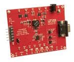

EVAL-ADM2491EEBZ
Analog Devices Inc.The ADM2491E is an isolated data transceiver with ?8 kV ESD protection and is suitable for high speed, half- or full-duplex communication on multipoint transmission lines. For half-duplex operation, the transmitter outputs and the receiver inputs share the same transmission line. Transmitter output Pin Y is linked externally to receiver input Pin A, and transmitter output Pin Z to receiver input Pin B.The ADM2491E is designed for balanced transmission lines and complies with ANSI TIA/EIA RS-485-A-1998 and ISO 8482: 1987(E). The device employs Analog Devices, Inc., iCoupler? technology to combine a 3-channel isolator, a threestate differential line driver, and a differential input receiver into a single packageThe differential transmitter outputs and receiver inputs feature electrostatic discharge circuitry that provides protection to ?8 kV using the human body model (HBM). The logic side of the device can be powered with either a 5 V or a 3.3 V supply, whereas the bus side requires an isolated 5 V supply.The device has current-limiting and thermal shutdown features to protect against output short circuits and situations where bus contention could cause excessive power dissipation.The ADM2491E is available in a wide body, 16-lead SOIC package and operates over the ?40?C to +85?C temperature range.Applications Isolated RS-485/RS-422 interfaces Industrial field networks INTERBUS Multipoint data transmission systems

ADL5604-EVALZ
Analog Devices Inc.The ADL5604 is a very broadband RF driver amplifier that operates over the wide frequency range of 700 MHz to 2700 MHz. The ADL5604 is also highly linear and has a very low power consumption, enabling the driver to be packaged in a compact 16-lead, 4 mm ? 4 mm LFCSP.For thermal management, the ADL5604 uses an exposed paddle, and the upper and lower pins of the package are all grounded, which gives the ADL5604 excellent thermal transfer characteristics.The ADL5604 can be quickly powered down or up in 50 ns for applications requiring TX shutdown, such as TDD systems.The ADL5604 operates on a single 5 V supply voltage and draws only 318 mA of supply current.The driver is fabricated on a GaAs HBT process and operates from ?40?C to +85?C. A fully populated evaluation board is available.

ADL5725-EVALZ
Analog Devices Inc.The ADL5725 is a narrow-band, high performance, low noise amplifier (LNA) targeting microwave radio link receiver designs. The monolithic silicon germanium (SiGe) design is optimized for microwave radio link bands ranging from 17.7 GHz to 19.7 GHz. The unique design offers a single-ended 50 ? input impedance and provides a 100 ? balanced differential output that is ideal for driving Analog Devices, Inc., differential downconverters and radio frequency (RF) sampling analog-to-digital converters (ADCs). This low noise amplifier provides noise figure performance that, in the past, required more expensive three-five (III-V) compounds process technology to achieve.The ADL5721 and ADL5723 to ADL5726 family of narrow-band LNAs are each packaged in a tiny, thermally enhanced, 2.00 mm ? 2 mm LFCSP package. The ADL5721 and ADL5723 to ADL5726 family operates over the temperature range of ?40?C to +85?C.Applications Point to point microwave radios Instrumentation Satellite communications (SATCOM) Phased arrays

ADL5802-EVALZ
Analog Devices Inc.The ADL5802 uses high linearity, double-balanced, active mixer cores with integrated LO buffer amplifiers to provide high dynamic range frequency conversion from 100 MHz to 6 GHz. The mixers benefit from a proprietary linearization architecture that provides enhanced input IP3 performance when subject to high input levels. A bias adjust feature allows the input linearity, SSB noise figure, and dc current to be optimized using a single control pin. The high input linearity allows the device to be used in demanding cellular applications where in-band blocking signals may otherwise result in degradation in dynamic performance. The balanced active mixer arrangement provides superb LO to RF and LO to IF leakage, typically better than ?30 dBm.The IF outputs are designed for a 200 ? source impedance and provide a typical voltage conversion gain of 7.6 dB when loaded into a 200 ? load.The ADL5802 is fabricated using a SiGe high performance IC process. The device is available in a compact 4 mm ? 4 mm, 24-lead LFCSP package and operates over a ?40?C to +85?C temperature range. An evaluation board is also available.APPLICATIONSCellular base station receiversMain and diversity receiver designsRadio link downconvertersData Sheet, Rev 0, 11/2009


ADL5902-EVALZ
Analog Devices Inc.The ADL5902 is a true rms responding power detector that hasa 65 dB measurement range when driven with a single-ended 50 ? source. This feature makes the ADL5902 frequencyversatile by eliminating the need for a balun or any other form of external input tuning for operation up to 9 GHz.The ADL5902 provides a solution in a variety of high frequencysystems requiring an accurate measurement of signal power. Requiring only a single supply of 5 V and a few capacitors, it is easy to use and capable of being driven single-ended or with abalun for differential input drive. The ADL5902 can operate from 50 MHz to 9 GHz and can accept inputs from ?62 dBm to at least +3 dBm with large crest factors, such as GSM, CDMA,W-CDMA, TD-SCDMA, WiMAX, and LTE modulated signals.The ADL5902 can determine the true power of a high frequency signal having a complex low frequency modulation envelope or can be used as a simple low frequency rmsvoltmeter. Used as a power measurement device, VOUT isconnected to VSET. The output is then proportional to thelogarithm of the rms value of the input. In other words, thereading is presented directly in decibels and is scaled 1.06 V per decade, or 53 mV/dB; other slopes are easily arranged. In controller mode, the voltage applied to VSET determines thepower level required at the input to null the deviation from the set point. The output buffer can provide high load currents.The ADL5902 has 1.5 mW power consumption when powereddown by a logic high applied to the PWDN pin. It powers up within approximately 5 ?s to its nominal operating current of 73 mA at 25?C. The ADL5902 is supplied in a 4 mm ? 4 mm,16-lead LFCSP for operation over the wide temperature rangeof ?40?C to +125?C.The ADL5902 is also pin-compatible with the AD8363, 50 dBdynamic range TruPwr? detector. This feature allows the designer to create one circuit layout for projects requiring different dynamic ranges. A fully populated RoHS-compliant evaluation board is available.Applications Power amplifier linearization/control loops Transmitter power controls Transmitter signal strength indication (TSSI) RF instrumentation


