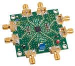
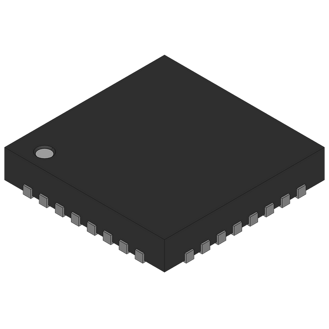
Top Manufacturers
Stock

Displaying 2201 - 2220 of 5453

Evaluation Kits from Analog Devices Inc.

LTC3805IMSE-5 Demo Board | SEPIC, 5V ≤ VIN ≤ 30V, VOUT = 12V @ 3A

Analog Devices Inc.
Demonstration circuit 1576 is high efficiency non-isolated SEPIC (Single Ended Primary Inductor Converter) converter featuring the LTC3805-5 switching controller. The DC1576 converts a 5V to 30V input to 12V at 3A of output current. The DC1576 can be easily modified to generate output voltages in the range from 0.8V to 48V.

LTC3108EDE-1 Demo Board | Ultralow Voltage Step-Up Converter and Power Manager

Analog Devices Inc.
DC1582B-B: Demo Board for the LTC3108-1 Ultralow Voltage Step-Up Converter and Power Manager.

LTC3625-1EDE Demo Board | VIN = 2.7V to 5.5V, VOUT = 4.5V or 4.0V @ IOUT up to 1A

Analog Devices Inc.
Demonstration circuit 1583A is a 1A high efficiency 2-Cell supercapacitor charger with automatic cell balancing featuring the LTC3625/LTC3625-1. The LTC3625/LTC3625-1 are step-up/step-down programmable supercapacitor chargers designed to charge two supercapacitors in series to a fixed voltage of 5.3V or 4.8V (LTC3625), or 4.5V or 4.0V (LTC3625-1) from a 2.7V to 5.5V input supply. Automatic cell balancing is achieved during the charging phase, preventing overvoltage damage to either supercapacitor while maximizing charge rate.

LTC3105EDD | 250mV Start-Up, Step-Up DC/DC Converter with Maximum Power Point Control

Analog Devices Inc.
Demonstration circuit 1587A is a boost converter optimized for relatively high impedance, very low voltage input power sources. It allows a user to quickly evaluate the LTC3105 boost converter and LDO regulator. Capable of operating with an input voltage as low as 250mV and as high as 5V, the circuit features maximum power point control (MPPC). Jumpers on the circuit board allow the user to select several MPPC voltages, three boost output voltages and three LDO regulator output voltages. Also included are jumpers for shutdown and for selecting an external pull-up voltage for the power good status output. Terminals are provided for input and output connections, power good output and external power good supply input, shutdown input, and provisions for external MPPC resistor and MPPC diode input. This demonstration board is especially designed for low power solar cell applications.

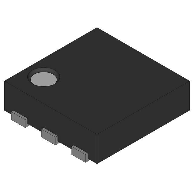
LTC2635-LMI12 | 12-Bit Quad I2C DAC (2.5V Internal Reference Mode, Reset to Mid-Scale), Requires DC590

Analog Devices Inc.
DC1593A-A: Demo Board for the LTC2635-12 Quad 12-Bit I2C VOUT DACs with 10ppm/°C Reference.
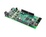
DC1594A-B

Analog Devices Inc.
The LTC4219 is an integrated solution for Hot Swap applications that allows a board to be safely inserted and removed from a live backplane. The part integrates a Hot Swap controller, power MOSFET and current sense resistor in a single package for small form factor applications. The LTC4219 provides separate inrush current control and a 10% accurate 5.6A current limit with foldback current limiting. The current limit threshold can be adjusted dynamically using an external pin. Additional features include a current monitor output that amplifies the sense resistor voltage for ground referenced current sensing and a MOSFET temperature monitor output. Thermal limit and power good monitoring are also provided. The power good detection level and foldback current limit profile are internally preset for 5V (LTC4219-5) and 12V (LTC4219-12) applications.Applications RAID Systems Server I/O Cards Industrial

LTC3112EDHD Demo Board

Analog Devices Inc.
Demonstration Circuit 1598A is a fixed frequency synchronous buck-boost converter with an extended input and output range. The unique 4-switch, single inductor architecture provides low noise and seamless operation from input voltages above, below, or equal to the output voltage. The LTC3112 features selectable PWM or Burst Mode operation, and an easily synchronizable oscillator. An output current monitor allows the load current to be controlled or monitored. The LTC3112 operates with a 2.7V to 15V input voltage range and a VOUT range from 2.5V to 14V. The demonstration board has been designed to operate with VIN from 2.7V to 15V and an output current up to 2.5A. For VIN < 5V, IOUT capability is reduced. VOUT is set to 5.0V.

LT1425CS | Isolated Flyback Converter, 5V to 15V Input, +/- 15V Output @ 60mA

Analog Devices Inc.
DC159A-B: Demo Board for the LT1425 Isolated Flyback Switching Regulators.

LTC6412, LTC2261-14 | 10MHz to 800MHz, 31dB Range Analog Controlled VGA

Analog Devices Inc.
DC1600A: Demo Board for the LTC6412 800MHz, 31dB Range Analog-Controlled VGA.

LTC4012CUF Demo Board | Multi-Chemistry 8A Buck Battery Charger with PowerPath Control

Analog Devices Inc.
Demonstration circuit 1614 features the LTC4012CUF, a multi-chemistry single battery charger controller with PowerPath™ control. The input supply voltage is 13.5V to 20V and is initially configured for a current limit of 10A. The charger float voltage is programmed by jumpers to support 1- to 4- series cells of both Li-Ion/Polymer and Li-iron phosphate (LiFePO4) at 4.2V/cell and 3.6V/cell, for a total of eight settings. The demo board is initially configured for constant-voltage charging of a 12.6V Li-Ion/ Polymer battery and constant-current charging at 8A, though current derating may be necessary due to certain operating conditions.

EV1HMC8073LP3D

Analog Devices Inc.
The HMC8073 is a 6-bit digital step attenuator (DSA), operating from 0.6 GHz to 3.0 GHz, that features 31.5 dB of attenuation range with 0.5 dB steps.The HMC8073 is implemented in a silicon process, offering a fast settling time, low power consumption, and high electrostatic discharge (ESD) robustness. The device features safe state transitions, allowing attenuation state changes without overshooting, and is optimized for excellent step accuracy and high power and high linearity over frequency and temperature range. The radio frequency (RF) input and output are internally matched to 50 ? and do not require any external matching components. The design is bidirectional, and the RF input and output are interchangeable.The external address feature of the HMC8073 allows users to control up to eight DSAs using a single bus. The DSA has an on-chip regulator that supports a wide supply operating range from 3.3 V to 5.0 V with no performance change in electrical characteristics. The HMC8073 incorporates a complementary metal-oxide semiconductor (CMOS)- and transistor transitory logic (TTL)- compatible interface that supports serial (3-wire) control of the attenuator.The HMC8073 comes in an RoHS compliant, compact, 3 mm ? 3 mm LFCSP package.Applications Cellular infrastructure Microwave radios? Very small aperture terminals Test equipment and sensors

EVAL-ADUC7039QSPZ

Analog Devices Inc.
The ADuC7039 is a complete system solution for battery monitoring in 12 V automotive applications. This device integrates all of the required features to precisely and intelligently monitor, process, and diagnose 12 V battery parameters including battery current, voltage, and temperature over a wide range of operating conditions.APPLICATIONS Battery sensing/management for automotive systems

EKIT01-HMC1033LP6G

Analog Devices Inc.
The HMC1033LP6GE is a low-noise, wide-band 3.3 V clock generator IC with a fractional-N Phase Locked Loop (PLL) that features an integrated Voltage Controlled Oscillator (VCO). The device provides differential clock outputs between 25 MHz and 550 MHz range. The HMC1033LP6GE features a low noise Phase Detector (PD) and Delta- Sigma modulator, capable of operating at up to 100 MHz which permits wider loop-bandwidths and excellent spurious performance.The HMC1033LP6GE features industry leading phase noise and jitter performance, across the operating range, that enable it to improve link level jitter performance, Bit-Error-Rates (BER) and eye diagram metrics. The superior noise floor (

EV-ADF4153SD1Z

Analog Devices Inc.
The ADF4153 is a fractional-N frequency synthesizer that implements local oscillators in the upconversion and downconversion sections of wireless receivers and transmitters. It consists of a low noise digital phase frequency detector (PFD), a precision charge pump, and a programmable reference divider. There is a ?-? based fractional interpolator to allow programmable fractional-N division. The INT, FRAC, and MOD registers define an overall N divider (N = (INT + (FRAC/MOD))). In addition, the 4-bit reference counter (R counter) allows selectable REFIN frequencies at the PFD input. A complete phase- locked loop (PLL) can be implemented if the synthesizer is used with an external loop filter and a voltage controlled oscillator (VCO).A simple 3-wire interface controls all on-chip registers. The device operates with a power supply ranging from 2.7 V to 3.3 V and can be powered down when not in use.Applications CATV equipment Base stations for mobile radio (GSM, PCS, DCS, WiMAX, SuperCell 3G, CDMA, W-CDMA) Wireless handsets (GSM, PCS, DCS, CDMA, W-CDMA) Wireless LANs, PMR Communications test equipment

EV-RPG2-ENZ

Analog Devices Inc.
The ADIN2299 is a complete, pretested solution that manages the industrial protocol and network traffic for an applications processor.The module contains everything needed to participate in a Ether-CAT, PROFINET? real-time (RT) and isochronous real time (IRT), EtherNet/IP network, including a communications controller, protocol stack, flash, RAM, follower controller, and physical layer (PHY). An applications processor connects via a universal asynchronousreceiver transmitter (UART), serial peripheral interface (SPI), or Ethernet interface.At the software layer, the applications processor connects to a unified interface so the supported industrial protocols can be used without changing the applications processor software. The ADIN2299 platform was precertified so that the field device can operate in any of the supported industrial Ethernet networks.PRODUCT HIGHLIGHTSMultiprotocol supportSmall form factor for embedded applicationsLow power and low latencyRobust network policing ensures passing PROFINET Netload Class 3APPLICATIONS Factory and process automation Motion control Building automation Transportation

DC2581A-A

Analog Devices Inc.
The LTC2341-18 is an 18-bit, low noise 2-channel simultaneous sampling successive approximation register (SAR) ADC with differential, wide common mode range inputs. Operating from a 5V supply and using the internal reference and buffer, both channels of this SoftSpan? ADC can be independently configured on a conversion-by-conversion basis to accept ?4.096V, 0V to 4.096V, ?2.048V, or 0V to 2.048V signals. One channel may also be disabled to increase throughput on the other channel.The wide input common mode range and 105dB CMRR of the LTC2341-18 analog inputs allow the ADC to directly digitize a variety of signals, simplifying signal chain design. This input signal flexibility, combined with ?4LSB INL, no missing codes at 18 bits, and 95dB SNR, makes the LTC2341-18 an ideal choice for many applications requiring wide dynamic range.The LTC2341-18 supports pin-selectable SPI CMOS (1.8V to 5V) and LVDS serial interfaces. Either one or two lanes of data output may be employed in CMOS mode, allowing the user to optimize bus width and throughput.Applications Programmable Logic Controllers Industrial Process Control Medical Imaging High Speed Data Acquisition

EV-ADF4159EB1Z

Analog Devices Inc.
The ADF4159 is a 13 GHz, fractional-N frequency synthesizer with modulation and both fast and slow waveform generation capability. The part uses a 25-bit fixed modulus, allowing subhertz frequency resolution.The ADF4159 consists of a low noise digital phase frequency detector (PFD), a precision charge pump, and a programmable reference divider. The ?-?-based fractional interpolator allows programmable fractional-N division. The INT and FRAC registers define an overall N divider as N = INT + (FRAC/225).The ADF4159 can be used to implement frequency shift keying (FSK) and phase shift keying (PSK) modulation. Frequency sweep modes are also available to generate various waveforms in the frequency domain, for example, sawtooth and triangular waveforms. Sweeps can be set to run automatically, or each step manually triggered by an external pulse. The ADF4159 features cycle slip reduction circuitry, which enables faster lock times without the need for modifications to the loop filter.Control of all on-chip registers is via a simple 3-wire interface. The ADF4159 operates with an analog power supply in the range of 2.7 V to 3.45 V and a digital power supply in the range of 1.62 V to 1.98 V. The device can be powered down when not in use.ApplicationsCommunications infrastructureCommunications test equipmentInstrumentationFMCW radars

Displaying 2201 - 2220 of 5453

Latest Parts

IN STOCK 13664
Buy

ASX00049

Arduino

* $43.32 - * $50.39

IN STOCK 2847
Buy

1687559

Phoenix Contact Ltd

[no prices available]

IN STOCK 2
Buy

Reference Designs

RD006

Wurth Elektronik

RD006 - 3 W Dual-output isolated auxiliary supply for communication interfaces and measurement systems

CN0583

Analog Devices Inc.

Multistandard Micropower Verified Smoke Detection System-on-Module

Technical Resources

EVALUATION KITS

EVAL-AD7124-8SDZ

Analog Devices Inc.

$0.00 - * $79.17

IN STOCK 792
Buy
View All