Top Manufacturers
MORE
Stock

Displaying 5181 - 5200 of 12850

Evaluation Kits

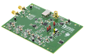
EV-ADF41513SD2Z

Analog Devices Inc.
The ADF41513 is an ultralow noise frequency synthesizer that can be used to implement local oscillators (LOs) as high as 26.5 GHz in the upconversion and downconversion sections of wireless receivers and transmitters.The ADF41513 is designed on a high performance silicon geranium (SiGe), bipolar complementary metal-oxide semiconductor (BiCMOS) process, achieving a normalized phase noise floor of ?235 dBc/Hz. The phase frequency detector (PFD) operates up to 250 MHz (integer N mode)/125 MHz (fractional-N mode) for improved phase noise and spur performance. The variable modulus, ?-? modulator allows extremely fine resolution when using a 49-bit divide value. The ADF41513 can be used as an integer N phase-locked loop (PLL), or it can be used as a fractional-N PLL with either a fixed modulus for subhertz frequency resolution or variable modulus for subhertz exact frequency resolution.A complete PLL is implemented when the synthesizer is used with an external loop filter and voltage controlled oscillator (VCO). The 26.5 GHz bandwidth eliminates the need for a frequency doubler or divider stage, simplifying system architecture and reducing cost. The ADF41513 is packaged in a compact, 24-lead, 4 mm ? 4 mm LFCSPApplications Test equipment and instrumentation Wireless infrastructure Microwave point to point and multipoint radios Very small aperture terminal (VSAT) radios Aerospace and defense

EV-ADF4156SD1Z

Analog Devices Inc.
The ADF4156 is a 6.2 GHz fractional-N frequency synthesizer that implements local oscillators in the up-conversion and down-conversion sections of wireless receivers and transmitters. It consists of a low noise digital phase frequency detector (PFD), a precision charge pump, and a programmable reference divider. There is a ??? based fractional interpolator to allow programmable fractional-N division. The INT, FRAC, and MOD registers define an overall N divider (N = (INT + (FRAC/MOD))). The RF output phase is programmable for applications that require a particular phase relationship between the output and the reference. The ADF4156 also features cycle slip reduction circuitry, leading to faster lock times without the need for modifications to the loop filter.Control of all on-chip registers is via a simple 3-wire interface. The device operates with a power supply ranging from 2.7 V to 3.3 V and can be powered down when not in use.ApplicationsCATV equipmentBase stations for mobile radio (WiMAX, GSM, PCS, DCS, SuperCell 3G, CDMA, WCDMA)Wireless handsets (GSM, PCS, DCS, CDMA, WCDMA)Wireless LANs, PMRCommunications test equipment

EV-ADF4193SD2Z

Analog Devices Inc.
The ADF4193 frequency synthesizer can be used to implement local oscillators in the upconversion and downconversion sections of wireless receivers and transmitters. Its architecture is specifically designed to meet the GSM/EDGE lock time requirements for base stations. It consists of a low noise, digital phase frequency detector (PFD), and a precision differential charge pump. There is also a differential amplifier to convert the differential charge pump output to a single-ended voltage for the external voltage-controlled oscillator (VCO).The ?-?-based fractional interpolator, working with the N divider, allows programmable modulus fractional-N division. Additionally, the 4-bit reference (R) counter and on-chip frequency doubler allow selectable reference signal (REFIN) frequencies at the PFD input. A complete phase-locked loop (PLL) can be implemented if the synthesizer is used with an external loop filter and a VCO. The switching architecture ensures that the PLL settles inside the GSM time slot guard period, removing the need for a second PLL and associated isolation switches. This decreases cost, complexity, PCB area, shielding, and characterization on previous ping-pong GSM PLL architectures.Applications GSM/EDGE base stations PHS base stations Instrumentation and test equipment

EV-ADF4355-2SD1Z

Analog Devices Inc.
The ADF4355-2 allows implementation of fractional-N or integer-N phase-locked loop (PLL) frequency synthesizers when used with an external loop filter and an external reference frequency. A series of frequency dividers permits operation from 54 MHz to 4400 MHz. The ADF4355-2 has an integrated VCO with a fundamental output frequency ranging from 3400 MHz to 6800 MHz. In addition, the VCO frequency is connected to divide by 1, 2, 4, 8, 16, 32, or 64 circuits that allow the user to generate RF output frequencies as low as 54 MHz. For applications that require isolation, the RF output stage can be muted. The mute function is both pin and software controllable.Control of all on-chip registers is through a simple 3-wire interface. The ADF4355-2 operates with analog and digital power supplies ranging from 3.15 V to 3.45 V, with charge pump and VCO supplies from 4.75 V to 5.25 V. The ADF4355-2 also contains hardware and software power-down modes.Applications Wireless infrastructure (W-CDMA, TD-SCDMA, WiMAX, GSM, PCS, DCS, DECT) Point to point/point to multipoint microwave links Satellites/VSATs Test equipment/instrumentation Clock generation

EV-ADF4356SD1Z

Analog Devices Inc.
The ADF4356 allows implementation of fractional-N or integer-N phase-locked loop (PLL) frequency synthesizers when used with an external loop filter and an external reference frequency. A series of frequency dividers at another frequency output permits operation from 53.125 MHz to 6800 MHz.The ADF4356 has an integrated VCO with a fundamental output frequency ranging from 3400 MHz to 6800 MHz. In addition, the VCO frequency is connected to divide by 1, 2, 4, 8, 16, 32, or 64 circuits that allow the user to generate RF output frequencies as low as 53.125 MHz. For applications that require isolation, the RF output stage can be muted. The mute function is both pin- and software-controllable.Control of all on-chip registers is through a simple 3-wire interface. The ADF4356 operates with analog and digital power supplies ranging from 3.15 V to 3.45 V, with charge pump and VCO supplies from 4.75 V to 5.25 V. The ADF4356 also contains hardware and software power-down modes.Applications Wireless infrastructure (LTE, W-CDMA, TD-SCDMA, WiMAX, GSM, PCS, DCS) Point to point/point to multipoint microwave links Satellites/VSATs Test equipment/instrumentation Clock generation

EV-ADF4360-0EB1Z

Analog Devices Inc.
The ADF4360-0 is a fully integrated integer-N synthesizer andvoltage controlled oscillator (VCO). The ADF4360-0 is designedfor a center frequency of 2600 MHz. In addition, a divide-by-2option is available, whereby the user gets an RF output of between 1200 MHz and 1360 MHz.Control of all the on-chip registers is through a simple 3-wireinterface. The device operates with a power supply ranging from3.0 V to 3.6 V and can be powered down when not in use.

EV-ADF4360-5EB1Z

Analog Devices Inc.
The ADF4360-5 is a fully integrated integer-N synthesizer andvoltage controlled oscillator (VCO). The ADF4360-5 is designedfor a center frequency of 1300 MHz. In addition, a divide-by-2option is available, whereby the user gets an RF output ofbetween 600 MHz and 700 MHz. Control of all the on-chip registers is through a simple 3-wire interface. The device operates with a power supply ranging from 3.0 V to 3.6 V and can be powered down when not in use.

EV-ADF4360-6EB1Z

Analog Devices Inc.
The ADF4360-6 is a fully integrated integer-N synthesizerand voltage-controlled oscillator (VCO). The ADF4360-6 isdesigned for a center frequency of 1150 MHz. In addition, adivide-by-2 option is available, whereby the user receives an RFoutput of between 525 MHz and 625 MHz.Control of all the on-chip registers is through a simple 3-wireinterface. The device operates with a power supply ranging from3.0 V to 3.6 V and can be powered down when not in use.Applications Wireless handsets (DECT, GSM, PCS, DCS, WCDMA) Test equipment Wireless LANs CATV equipment

EV-ADF70301-169BZ

Analog Devices Inc.
The ADF7030-1 is a fully integrated, radio transceiver achieving high performance at very low power. The ADF7030-1 is ideally suited for applications that require long range, network robustness, and long battery life. It is suitable for applications that operate in the ISM, SRD, and licensed frequency bands at 169.4 MHz to 169.6 MHz, 426 MHz to 470 MHz, and 863 MHz to 960 MHz. It provides extensive support for standards-based protocols like IEEE802.15.4g while also providing flexibility to support a wide range of proprietary protocols.The highly configurable low intermediate frequency (IF) receiver supports a large range of receiver channel bandwidths from 2.6 kHz to 406 kHz. This range of receiver channel bandwidths allows the ADF7030-1 to support ultranarrow-band, narrow-band, and wideband channel spacing.The ADF7030-1 features two independent PAs supporting output power ranges of ?20 dBm to +13 dBm and ?20 dBm to +17 dBm. The PAs support ultrafine adjustment of the power with a step resolution of 0.1 dB. The PA output power is exceptionally robust over temperature and voltage. The PAs have an automatic power ramp control to limit spectral splatter to meet regulatory standards.The ADF7030-1 features an on-chip ARM??Cortex?-M0 processor that performs radio control, radio calibration, and packet management. Cortex-M0 eases the processing burden of the host processor because the ADF7030-1 integrates the lower layers of a typical communication protocol stack. This internal processor also permits the download and execution of Analog Devices, Inc., provided firmware modules that can extend the functionality of the ADF7030-1.The ADF7030-1 has two packet modes: generic packet mode and IEEE802.15.4g mode. In generic packet mode, the packet format is highly flexible and fully programmable, thereby ensuring its compatibility with proprietary packet formats. In IEEE802.15.4g packet mode, the packet format conforms to the?IEEE802.15.4g standard. FEC, as per the IEEE802.15.4g standard, is also supported.The ADF7030-1 operates with a power supply range of 2.2 V to 3.6 V and has very low power consumption in both Tx and Rx modes, enabling long lifetimes in battery-operated systems. An ultralow power deep sleep mode achieves a typical current of 10 nA with the configuration memory retained.A complete wireless solution can be built using a small number of external discrete components and a host processor (typically a microcontroller). The host processor can configure the ADF7030-1 using a simple command-based protocol over a standard 4-wire SPI interface. A single-byte command transitions the radio between states or performs a radio function.The ADF7030-1 is available in two package types: a 6 mm ? 6 mm, 40-lead LFCSP and a 7 mm ? 7 mm, 48-lead LQFP. Both package types use NiPdAu plating to mitigate against silver migration in high humidity applications. The ADF7030-1 operating temperature range is ?40?C to +85?C.For Figure 13 to Figure 19, Figure 30, Figure 42, Figure 60, Figure 61, and Figure 75 in the Typical Performance Characteristics section, PA_COARSE is a programmable value that provides a coarse adjustment of the PA output power. This value can be programmed in the range of 1 to 6 for PA1, and from 1 to 10 for PA2. PA_FINE is a programmable value that provides a fine adjustment of the PA output power. This value can be programmed in the range of 3 to 127 for both PA1 and PA2. PA_MICRO is a programmable value that provides a microadjustment (typically

EVAL-ADSW4000KTZ

Analog Devices Inc.
The ADSW4000 ADI EagleEye? PeopleCount algorithm enables a people counting function within internal spaces, such as meeting rooms or office spaces. The system edge node analytics unlocks informed insights and analytics with an accurate and secure people counting capability. This data can provide the insight to improve asset and people management, social distancing, security, employee engagement, space utilization, labor productivity, and energy efficiency.The ADSW4000 is designed to operate solely with the Analog Devices, Inc., ADSP-BF707 Blackfin+? core embedded processor (ADSPBF707BBCZ4-EGE) and is optimized for a CMOS 2D video graphics array (VGA) sensor and lens (the recommended Chicony CYFI013 module incorporates an ON Semiconductor? ASX340AT3C00XPED0-DPBR CMOS image sensor, Chicony YT70005 lens, and lens holder with infrared (IR) filter).The ADSW4000 ADI EagleEye? PeopleCount algorithm provides up to a 90% accurate people count within the target area.The following are the accuracies achieved for tested radii from 3 m to 5 m:90% accuracy in 3 m radius85% accuracy in 4 m radius80% accuracy in 5 m radiusAPPLICATIONSBuilding technology solutionsIntelligent buildingsOccupancy analyticsBuilding management systems

EVAL-ADT7301EBZ

Analog Devices Inc.
The ADT7301 is a complete temperature monitoring system in SOT-23 and MSOP packages. It contains a band gap temperature sensor and a 13-bit ADC to monitor and digitize the temperature reading to a resolution of 0.03125?C.The ADT7301 has a flexible serial interface that allows easy interfacing to most microcontrollers. The interface is compatible with SPI?, QSPI and MICROWIRE? protocol and is also compatible with DSPs. The part features a standby mode that is controlled via the serial interface. The ADT7301's wide supply voltage range, low supply current and SPI-compatible interface, make it ideal for a variety of applications, including personal computers, office equipment, automotive and domestic appliances. TheADT7301 is rated for operation over the ?40?C to +150?Ctemperature range. It is not recommended to operate the deviceat temperatures above +125?C for greater than a total of 5% (5,000 hours) of the lifetime of the device. Exposure beyond thislimit affects device reliability.PRODUCT HIGHLIGHTS On-chip temperature sensor that allows an accurate measurement of the ambient temperature. The measurable temperature range is ?40?C to +150?C. Supply voltage of 2.7 V to 5.25 V. Space-saving 6-lead SOT-23 and 8-lead MSOP packages. Typical temperature accuracy of ?0.5?C. 13-bit temperature reading to 0.03125?C resolution. Shutdown mode that reduces the power consumption to 4.88 ?W with VDD = 3.3 V @ 1 SPS. Compatible with AD7814.APPLICATIONS Medical equipment Automotive Environmental controls Oil Temperature Hydraulic systems Cellular phones Hard disk drives Personal computers Electronic test equipment Office equipment Domestic appliances Process control

EVAL-ADT7410MBZ

Analog Devices Inc.
The ADT7410 is a high accuracy digital temperature sensor in anarrow SOIC package. It contains a band gap temperature referenceand a 13-bit ADC to monitor and digitize the temperature to a0.0625?C resolution. The ADC resolution, by default, is set to13 bits (0.0625?C). This can be changed to 16 bits (0.0078?C) bysetting Bit 7 in the configuration register (Register Address 0x03).The ADT7410 is guaranteed to operate over supply voltages from2.7 V to 5.5 V. Operating at 3.3 V, the average supply current is typically210 ?A. The ADT7410 has a shutdown mode that powersdown the device and offers a shutdown current of typically 2 ?A.The ADT7410 is rated for operation over the ?55?C to +150?Ctemperature range.Pin A0 and Pin A1 are available for address selection, giving theADT7410 four possible I2C addresses. The CT pin is an open-drainoutput that becomes active when the temperature exceedsa programmable critical temperature limit. The default criticaltemperature limit is 147?C. The INT pin is also an open-drainoutput that becomes active when the temperature exceeds aprogrammable limit. The INT and CT pins can operate in eithercomparator or interrupt mode.Applications Medical equipment Environmental control systems Computer thermal monitoring Thermal protection Industrial process control Power system monitors Hand-held applications

EVAL-ADUC7020MKZ

Analog Devices Inc.
The ADuC7019?/?ADuC7020?/ ADuC7021 /?ADuC7022?/?ADuC7024?/?ADuC7025?/ ADuC7026?/?ADuC7027?/?ADuC7028?/?ADuC7029 are fully integrated,1 MSPS, 12-bit data acquisition systems incorporating highperformance multichannel ADCs, 16-bit/32-bit MCUs, andFlash?/EE memory on a single chip.The ADC consists of up to 12 single-ended inputs. An additionalfour inputs are available but are multiplexed with the four DACoutput pins. The four DAC outputs are available only on certainmodels (ADuC7020, ADuC7026, ADuC7028, and ADuC7029).However, in many cases where the DAC outputs are not present,these pins can still be used as additional ADC inputs, giving amaximum of 16 ADC input channels. The ADC can operate insingle-ended or differential input mode. The ADC input voltageis 0 V to VREF. A low drift band gap reference, temperature sensor,and voltage comparator complete the ADC peripheral set.Depending on the part model, up to four buffered voltageoutput DACs are available on-chip. The DAC output range isprogrammable to one of three voltage ranges.The devices operate from an on-chip oscillator and a PLLgenerating an internal high frequency clock of 41.78 MHz(UCLK). This clock is routed through a programmable clockdivider from which the MCU core clock operating frequencyis generated. The microcontroller core is an ARM7TDMI?,16-bit/32-bit RISC machine, which offers up to 41 MIPS peakperformance. Eight kilobytes of SRAM and 62 kilobytes ofnonvolatile Flash/EE memory are provided on-chip. TheARM7TDMI core views all memory and registers as a singlelinear array.On-chip factory firmware supports in-circuit serial downloadvia the UART or I2C serial interface port; nonintrusive emulationis also supported via the JTAG interface. These features areincorporated into a low cost QuickStart? development systemsupporting this MicroConverter? family.The parts operate from 2.7 V to 3.6 V and are specified over anindustrial temperature range of ?40?C to +125?C. Whenoperating at 41.78 MHz, the power dissipation is typically120 mW. The ADuC7019 / ADuC7020 / ADuC7021 /? ADuC7022 / ADuC7024 / ADuC7025 / ADuC7026 / ADuC7027 / ADuC7028 / ADuC7029 areavailable in a variety of memory models and packages (seeOrdering Guide).APPLICATIONS Industrial control and automation systems Smart sensors, precision instrumentation Base station systems, optical networking

EVAL-ADUC7020QSZ

Analog Devices Inc.
The ADuC7019?/?ADuC7020?/ ADuC7021 /?ADuC7022?/?ADuC7024?/?ADuC7025?/ ADuC7026?/?ADuC7027?/?ADuC7028?/?ADuC7029 are fully integrated,1 MSPS, 12-bit data acquisition systems incorporating highperformance multichannel ADCs, 16-bit/32-bit MCUs, andFlash?/EE memory on a single chip.The ADC consists of up to 12 single-ended inputs. An additionalfour inputs are available but are multiplexed with the four DACoutput pins. The four DAC outputs are available only on certainmodels (ADuC7020, ADuC7026, ADuC7028, and ADuC7029).However, in many cases where the DAC outputs are not present,these pins can still be used as additional ADC inputs, giving amaximum of 16 ADC input channels. The ADC can operate insingle-ended or differential input mode. The ADC input voltageis 0 V to VREF. A low drift band gap reference, temperature sensor,and voltage comparator complete the ADC peripheral set.Depending on the part model, up to four buffered voltageoutput DACs are available on-chip. The DAC output range isprogrammable to one of three voltage ranges.The devices operate from an on-chip oscillator and a PLLgenerating an internal high frequency clock of 41.78 MHz(UCLK). This clock is routed through a programmable clockdivider from which the MCU core clock operating frequencyis generated. The microcontroller core is an ARM7TDMI?,16-bit/32-bit RISC machine, which offers up to 41 MIPS peakperformance. Eight kilobytes of SRAM and 62 kilobytes ofnonvolatile Flash/EE memory are provided on-chip. TheARM7TDMI core views all memory and registers as a singlelinear array.On-chip factory firmware supports in-circuit serial downloadvia the UART or I2C serial interface port; nonintrusive emulationis also supported via the JTAG interface. These features areincorporated into a low cost QuickStart? development systemsupporting this MicroConverter? family.The parts operate from 2.7 V to 3.6 V and are specified over anindustrial temperature range of ?40?C to +125?C. Whenoperating at 41.78 MHz, the power dissipation is typically120 mW. The ADuC7019 / ADuC7020 / ADuC7021 /? ADuC7022 / ADuC7024 / ADuC7025 / ADuC7026 / ADuC7027 / ADuC7028 / ADuC7029 areavailable in a variety of memory models and packages (seeOrdering Guide).APPLICATIONS Industrial control and automation systems Smart sensors, precision instrumentation Base station systems, optical networking

EVAL-ADUC7023QSPZ

Analog Devices Inc.
The ADuC7023 is a fully integrated, 1 MSPS, 12-bit data acquisition system, incorporating high performance multichannel ADCs, 16-bit/32-bit MCUs, and Flash/EE memory on a single chip.The ADC consists of up to 12 single-ended inputs. An additional four inputs are available but are multiplexed with the four DAC output pins. The ADC can operate in single-ended or differential input modes. The ADC input voltage is 0 V to VREF. A low drift band gap reference, temperature sensor, and voltage comparator complete the ADC peripheral set.The DAC output range is programmable to one of two voltage ranges. The DAC outputs have an enhanced feature of being able to retain their output voltage during a watchdog or software reset sequence.The devices operate from an on-chip oscillator and a PLL, generating an internal high frequency clock of 41.78 MHz. This clock is routed through a programmable clock divider from which the MCU core clock operating frequency is generated. The microcontroller core is an ARM7TDMI?, 16-bit/32-bit RISC machine that offers up to 41 MIPS peak performance. Eight kilobytes of SRAM and 62 kilobytes of nonvolatile Flash/EE memory are provided on chip. The ARM7TDMI core views all memory and registers as a single linear array.The ADuC7023 contains an advanced interrupt controller. The vectored interrupt controller (VIC) allows every interrupt to be assigned a priority level. It also supports nested interrupts to a maximum level of eight per IRQ and FIQ. When IRQ and FIQ interrupt sources are combined, a total of 16 nested interrupt levels are supported.On-chip factory firmware supports in-circuit download via the I2C serial interface port, and non-intrusive emulation is supported via the JTAG interface. These features are incorporated into a low cost QuickStart? development system supporting this MicroConverter? family. The part contains a 16-bit PWM with five output signals.For communication purposes, the part contains 2 ? I2C channels that can be individually configured for master or slave mode. An SPI interface supporting both master and slave modes is also provided.The parts operate from 2.7 V to 3.6 V and are specified over an industrial temperature range of ?40?C to +125?C. The ADuC7023 is available in either a 32-lead or 40-lead LFCSP package. A 36-ball wafer level CSP package (WLCSP) is also available.Applications Optical networking Industrial control and automation systems Smart sensors, precision instrumentation Base station systems

EVAL-ADUC7120QSPZ

Analog Devices Inc.
The ADuC7120/ADuC7121 are fully integrated, 12-bit, 1 MSPS, data acquisition systems incorporating a high performance multichannel ADC, 16-bit/32-bit microcontroller unit (MCU), and Flash?/EE memory on a single chip.The analog-to-digital converter (ADC) consists of eleven single-ended inputs for the ADuC7120 (seven single-ended inputs for the ADuC7121) and two extra differential input pairs. The two differential input pairs can be routed through a programmable gain amplifier (PGA). The ADC can operate in single-ended or differential input mode. The ADC input voltage is 0 V to VREF. A low drift band gap reference, temperature sensor, and voltage comparator complete the ADC peripheral set.The ADuC7120/ADuC7121 provide five current output digital-to-analog converters (DACs). The current sources (five current DACs) feature low noise and low drift, high-side current output at an 11-bit resolution. The five current digital-to-analog converters (IDACs) are as follows: IDAC0 with 250 mA full-scale (FS) output, IDAC1 with 200 mA FS output, IDAC2 with 45 mA FS output, IDAC3 with 80 mA FS output, and IDAC4 with 20 mA FS output.The ADuC7120/ADuC7121 also contain up to 12 voltage output DACs. The DAC output range is programmable to one of three voltage ranges.The devices operate from an on-chip oscillator and a phase-locked loop (PLL) generating an internal high frequency clock of 41.78 MHz (UCLK). This clock is routed through a programmable clock divider from which the MCU core clock operating frequency is generated. The microcontroller core is an ARM7TDMI?, 16-bit/32-bit reduced instruction set computer (RISC) machine, which offers up to 41 MIPS peak performance. 8 kB of SRAM and 126 kB of nonvolatile Flash/EE memory are provided on chip. The ARM7TDMI core views all memory and registers as a single linear array.On-chip factory firmware supports in circuit serial download via the I2C serial interface port; nonintrusive emulation is also supported via the JTAG interface. These features are incorporated into a low cost QuickStart development system supporting this MicroConverter? family.The devices operate from 3.0 V to 3.6 V, and they are specified over the ?40?C to +105?C industrial temperature range. The IDACs are powered from a separate input power supply, PVDD. When operating at 41.78 MHz, the power dissipation is typically 120 mW. The ADuC7120/ADuC7121 are available in a 108-ball chip-scale package ball grid array [CSP_BGA].Applications Optical modules?tunable laser

EVAL-ADUC814QSZ

Analog Devices Inc.
The ADuC814 MicroConverter? is a fully integrated 12-bit data acquisition system-on-a-chip. Like all of ADI's MicroConverter products, it features precision A/D & D/A conversion and a Flash microcontroller on a single chip.The ADuC814 is available in a 28-pin TSSOP package and operates on a 3V or 5V power supply.

EVAL-ADUC841QSZ

Analog Devices Inc.
The ADuC841/ADuC842/ADuC843 are complete smart transducer front ends, that integrates a high performance self-calibrating multichannel ADC, a dual DAC, and an optimized single-cycle 20 MHz 8-bit MCU (8051 instruction set compatible)on a single chip.The ADuC841 and ADuC842 are identical with the exception of the clock oscillator circuit; the ADuC841 is clocked directly from an external crystal up to 20 MHz whereas the ADuC842 uses a 32 kHz crystal with an on-chip PLL generating a programmable core clock up to 16.78 MHz.The ADuC843 is identical to the ADuC842 except that the ADuC843 has no analog DAC outputs.The microcontroller is an optimized 8052 core offering up to 20 MIPS peak performance. Three different memory options are available offering up to 62 kBytes of nonvolatile Flash/EE program memory. Four kBytes of nonvolatile Flash/EE data memory, 256 bytes RAM, and 2 kBytes of extended RAM are also integrated on-chip. The parts also incorporate additional analog functionality with two 12-bit DACs, power supply monitor, and a band gap reference. On-chip digital peripherals include two 16-bit ?-?. DACs, a dual output 16-bit PWM, a watchdog timer, a time interval counter, three timers/counters, and three serial I/O ports (SPI, I2C, and UART).On the ADuC812 and the ADuC832, the I2C and SPI interfaces share some of the same pins. For backwards compatibility, this is also the case for the ADuC841/ADuC842/ADuC843.However, there is also the option to allow SPI operate separately on P3.3, P3.4, and P3.5, while I2C uses the standard pins. The I2C interface has also been enhanced to offer repeated start, general call, and quad addressing.On-chip factory firmware supports in-circuit serial download and debug modes (via UART) as well as single-pin emulation mode via the EA pin..Applications Optical networking?laser power control Base station systems Precision instrumentation, smart sensors Transient capture systems DAS and communications systems

EVAL-ADUCM430ARDZ

Analog Devices Inc.
APPLICATIONS Optical networking?100G/200G/400G and higher frequency modulesFor more information on the ADuCM430, contact InfoOpticalNetwork@analog.com.

EVAL-ADUM1250EBZ

Analog Devices Inc.
The ADuM1250 /?ADuM1251 are hot swappable digital isolators with non-latching, bidirectional communication channels compatible with I2C interfaces. This eliminates the need for splitting I2C signals into separate transmit and receive signals for use with standalone optocouplers.The ADuM1250 provides two bidirectional channels, supporting a complete isolated I2C interface. The ADuM1251 provides one bidirectional channel and one unidirectional channel for those applications where a bidirectional clock is not required.Both the ADuM1250 and ADuM1251 contain hot swap circuitry to prevent glitching data when an unpowered card is inserted onto an active bus.These isolators are based on iCoupler? chip scale transformer technology from Analog Devices, Inc. iCoupler is a magnetic isolation technology with functional, performance, size, and power consumption advantages as compared to optocouplers. With the ADuM1250 / ADuM1251, iCoupler channels can be integrated with semiconductor circuitry, which enables a complete isolated I2C interface to be implemented in a small form factor.APPLICATIONS Isolated I2C, SMBus, or PMBus interfaces Multilevel I2C interfaces Power supplies Networking Power over Ethernet Hybrid electric vehicle battery management

Displaying 5181 - 5200 of 12850

Latest Parts

IN STOCK 13664
Buy

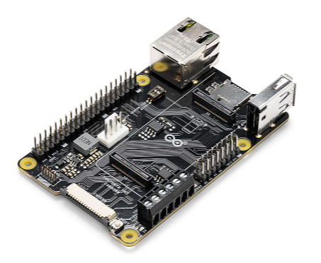
ASX00049

Arduino

* $43.36 - * $50.36

IN STOCK 2847
Buy

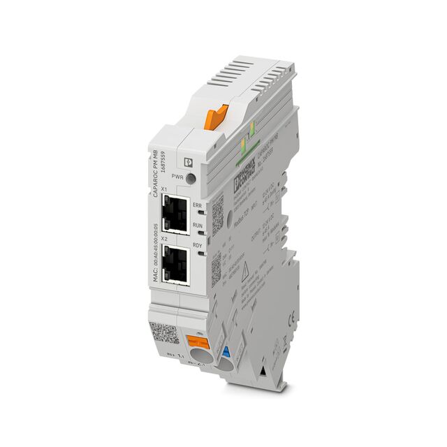
1687559

Phoenix Contact Ltd

[no prices available]

IN STOCK 2
Buy

Reference Designs

RD006

Wurth Elektronik

RD006 - 3 W Dual-output isolated auxiliary supply for communication interfaces and measurement systems

CN0583

Analog Devices Inc.

Multistandard Micropower Verified Smoke Detection System-on-Module

Technical Resources

EVALUATION KITS

EVAL-AD7124-8SDZ

Analog Devices Inc.

$0.00 - * $79.12

IN STOCK 792
Buy
View All