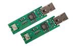
EVAL_PAN1323
Panasonic Industrial DevicesBluetooth Development Tools - 802.15.1 PAN1323 Evaluation Kit
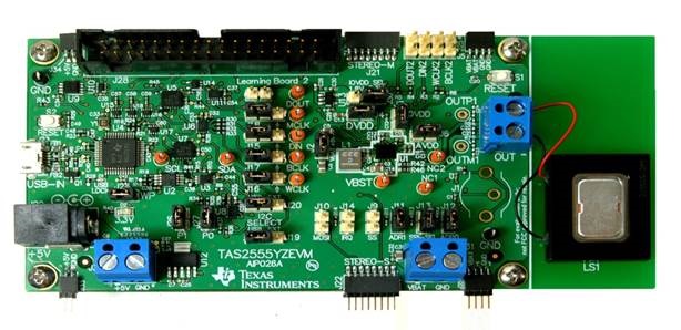
TAS2555 5.7W Class-D Audio Amplifier Evaluation Module
Texas InstrumentsTAS2555 5.7W Class-D Audio Amplifier Evaluation Module

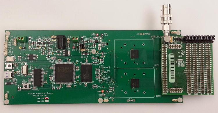
DDC1128 Evaluation Module for 128-Channel Current-Input Analog-to-Digital Converter
Texas InstrumentsDDC1128 Evaluation Module for 128-Channel Current-Input Analog-to-Digital Converter
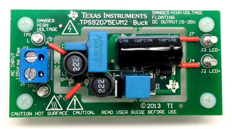
Non-Isolated; Phase Dimmable; Buck PFC LED Driver Evaluation Module
Texas InstrumentsNon-Isolated; Phase Dimmable; Buck PFC LED Driver Evaluation Module
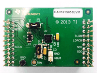
16-bit 1 Channel Digital to Analog Converter Evaluation Module
Texas Instruments16-bit 1 Channel Digital to Analog Converter Evaluation Module
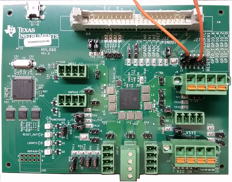
TPS659037 Power Management IC Evaluation Module
Texas InstrumentsTPS659037 Power Management IC Evaluation Module
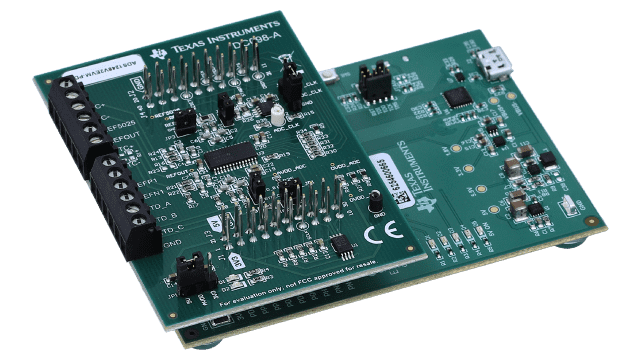
ADS1248 performance demonstration kit for 24-bit; 2-kSPS; eight-channel delta-sigma ADC
Texas InstrumentsADS1248 performance demonstration kit for 24-bit; 2-kSPS; eight-channel delta-sigma ADC
Bq34z100EVM 1s to 16s Impedance Track Fuel Gauge Battery Evaluation Module | Gas Gauge Battery
Texas InstrumentsBq34z100EVM 1s to 16s Impedance Track Fuel Gauge Battery Evaluation Module | Gas Gauge Battery
TPS548D22 DCAP3 High Performance; 40-A Single Synchronous Step-Down Converter Evaluation Module
Texas InstrumentsTPS548D22 DCAP3 High Performance; 40-A Single Synchronous Step-Down Converter Evaluation Module


