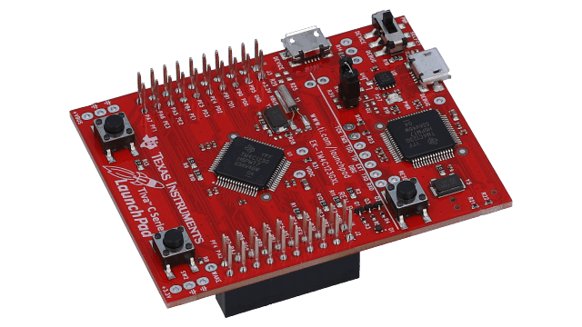
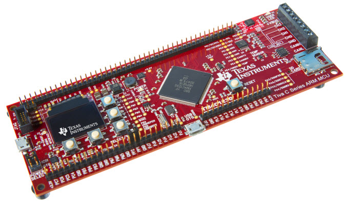
ARM® Cortex®-M4F Based MCU TM4C123G LaunchPad™ Evaluation Kit
Texas InstrumentsARM® Cortex®-M4F Based MCU TM4C123G LaunchPad™ Evaluation Kit
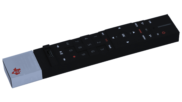
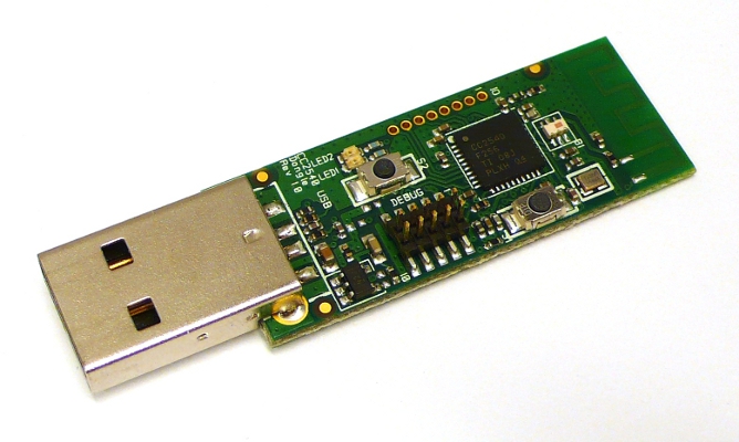
SimpleLink™ Bluetooth® low energy/ZigBee® RF4CE™ CC2650 remote control
Texas InstrumentsSimpleLink™ Bluetooth® low energy/ZigBee® RF4CE™ CC2650 remote control
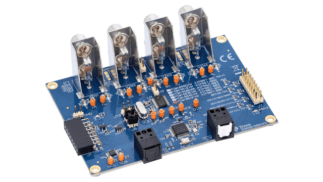
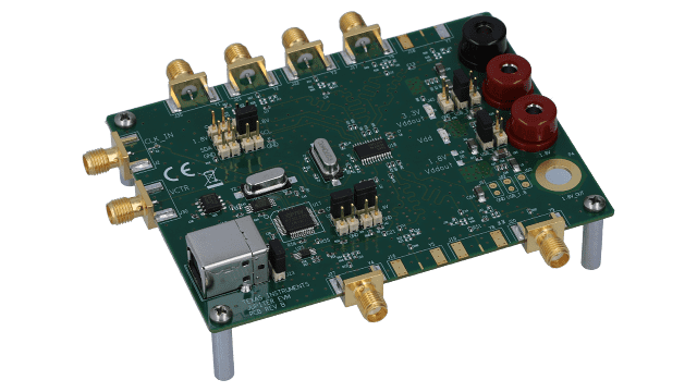
PCM1865 110dB 4-Ch Software-Controlled Audio ADC With Universal Front End Evaluation Module
Texas InstrumentsPCM1865 110dB 4-Ch Software-Controlled Audio ADC With Universal Front End Evaluation Module
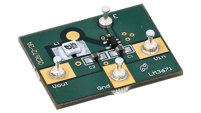
2MHz; 600mA Step-Down DC-DC Converter in SOT23-5 and 5-Bump Micro SMD
Texas Instruments2MHz; 600mA Step-Down DC-DC Converter in SOT23-5 and 5-Bump Micro SMD
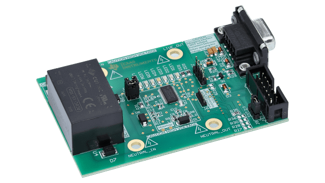
MSP430I240 evaluation board for sub metering
Texas InstrumentsMSP430I240 evaluation board for sub metering
Bluetooth Low Energy and proprietary wireless MCU
Texas InstrumentsBluetooth Low Energy and proprietary wireless MCU
Evaluation Module for BQ24170 1.6-MHz Synchronous Switch-Mode Li-Ion and Li-Polymer Battery Charger
Texas InstrumentsEvaluation Module for BQ24170 1.6-MHz Synchronous Switch-Mode Li-Ion and Li-Polymer Battery Charger
Single op-amp evaluation module for SO-8 (non-inverting) package
Texas InstrumentsSingle op-amp evaluation module for SO-8 (non-inverting) package
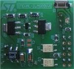
STEVAL-ILM001V1
STMicroelectronicsPlug-in Module for STM8S-DISCOVERY Interface for DALI Communication
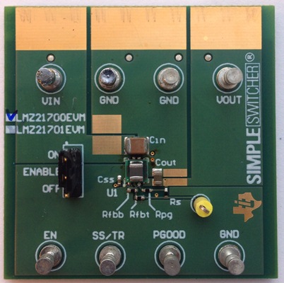
LMZ21700 650mA SIMPLE SWITCHER® Nano Module Evaluation Board
Texas InstrumentsLMZ21700 650mA SIMPLE SWITCHER® Nano Module Evaluation Board
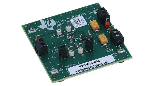
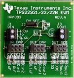
Evaluation Module for TPS2066C Dual-Channel; Current-Limited; Power-Distribution Switch
Texas InstrumentsEvaluation Module for TPS2066C Dual-Channel; Current-Limited; Power-Distribution Switch
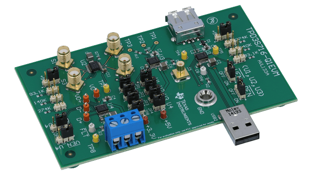
TPD3S716-Q1 Automotive USB 2.0 Interface Protection With Adjustable Current Limit Evaluation Module
Texas InstrumentsTPD3S716-Q1 Automotive USB 2.0 Interface Protection With Adjustable Current Limit Evaluation Module


