
Search results
D61C
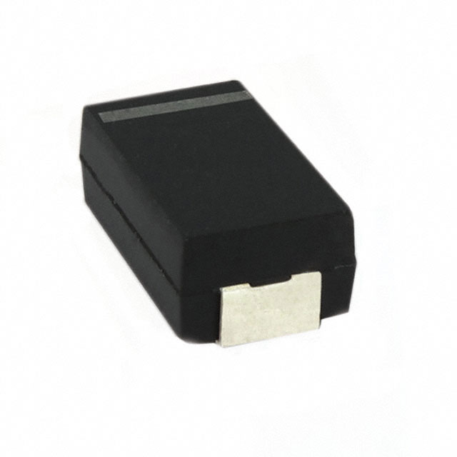
Murata Electronics (UK) Ltd.
From $0.94 • 1 k+ units available from DigiKey
D61C
Murata Electronics (UK) Ltd.
100 µF 16 V Aluminum - Polymer Capacitors 2917 (7343 Metric) 12mOhm 2000 Hrs @ 105°C
| Distributor | SKU | Stock | MOQ | 1 | 10 | 50 | 100 | 1,000 | 10,000 | |
|---|---|---|---|---|---|---|---|---|---|---|
| DigiKey | 490-ECASD61C107M012KA0DKR-ND | 5,448 | $2.46 | $1.89 | $1.73 | $1.44 | $1.01 | $0.94 | Buy |


Small and Simple Isolated Flyback Universal Vin: 5.2V@200mA: Primary-side Regulated Reference Design

Texas Instruments
Small and Simple Isolated Flyback Universal Vin: 5.2V@200mA: Primary-side Regulated Reference Design
Texas Instruments
Design features low component count and low cost isolated flyback: converting the universal mains (85Vac…275Vac) to 5.2V@200mA. Due to primary side regulation of the controller UCC28700: no optocoupler is needed to close the loop.
Adjacent Channel Power Ratio (ACPR) and Error Vector Magnitude (%EVM) Measurements

Texas Instruments
Adjacent Channel Power Ratio (ACPR) and Error Vector Magnitude (%EVM) Measurements
Texas Instruments
This reference design discusses the use of the TSW3085EVM with the TSW3100 pattern generator to test adjacent channel power ratio (ACPR) and error vector magnitude (EVM) measurements of LTE baseband signals. By using the TSW3100 LTE GUI: patterns are loaded into the TSW3085EVM which is comprised of the DAC3482: TRF3705: and LMK04806.
Interfacing the TLC5510 Analog-to-Digital Converter to the TMS320C203 DSP

Texas Instruments
Interfacing the TLC5510 Analog-to-Digital Converter to the TMS320C203 DSP
Texas Instruments
This application report presents guidelines for interfacing the Texas Instruments (TI(TM)) TLC5510 8-bit parallel-output analog-to-digital converter (ADC) to the TI TMS320C203 DSP data bus. The 8-bit ADC operates at a rate of 20 MHz. The C callable application program (assembly code) used to initialize the TMS320C203 and execute the code is also discussed.This report serves as reference inform
ADL8150-EVALZ

Analog Devices Inc.
ADL8150-EVALZ
Analog Devices Inc.
The ADL8150 is a self biased gallium arsenide (GaAs), monolithic microwave integrated circuit (MMIC), heterojunction bipolar transistor (HBT), low phase noise amplifier that operates from 6 GHz to 14 GHz. The amplifier provides 12 dB of typical signal gain, 18 dBm output power at 1 dB gain compression (OP1dB), and a typical output third-order intercept (OIP3) of 30 dBm. The amplifier requires 74 mA from a 5 V collector supply voltage. The ADL8150 also features inputs and outputs (I/Os) that are internally matched to 50 ?, and facilitates integration into multichip modules (MCMs). Note that throughout the data sheet, multifunction pins, such as RFOUT/VCC, are referred to either by the entire pin name or by a single function of the pin, for example, RFOUT, when only that function is relevant.Applications Military and space Test instrumentation Communications
ADP1051DC1-EVALZ

Analog Devices Inc.
ADP1051DC1-EVALZ
Analog Devices Inc.
The ADP1051 is an advanced digital controller with a PMBus? interface targeting high density, high efficiency dc-to-dc power conversion. This controller implements voltage mode control with high speed, input line feedforward for enhanced transient and improved noise performance. The ADP1051 has six programmable pulse-width modulation (PWM) outputs capable of controlling most high efficiency power supply topologies, with added control of synchronous rectification (SR). The device includes adaptive dead time compensation to improve efficiency over the load range, and programmable light load mode operation, combined with low power consumption, to reduce system standby power losses.The ADP1051 implements several features to enable a robust system of parallel and redundant operation for customers that require high availability or parallel connection. The device provides synchronization, reverse current protection, pre-bias startup, accurate current sharing between power supplies, and conditional overvoltage techniques to identify and safely shut down an erroneous power supply in parallel operation mode.The ADP1051 implements several features to enable a robust system of parallel and redundant operation for customers that require high availability or parallel connection. The device provides synchronization, reverse current protection, pre-bias startup, accurate current sharing between power supplies, and conditional overvoltage techniques to identify and safely shut down an erroneous power supply in parallel operation mode.APPLICATIONS High density, isolated DC/DC power supplies Intermediate bus converters High availability parallel power systems Server, storage, industrial, networking, and communications infrastructure
How TMS320 Tools Interact With the TMS320C32's Enhanced Memory Interface
Texas Instruments
How TMS320 Tools Interact With the TMS320C32's Enhanced Memory Interface
Texas Instruments
This document describes using the TMS320 floating-point digital signal processor (DSP) optimizing C compiler and assembly language tools with the variable memory width and data sizes supported by the
JESD204B Link Latency Design Using a High Speed ADC

Texas Instruments
JESD204B Link Latency Design Using a High Speed ADC
Texas Instruments
JESD204B links are the latest trend in data-converter digital interfaces. These links take advantage of high-speed serial-digital technology to offer many compelling benefits including improved channel densities. This reference design addresses one of the challenges of adopting the new interface: understanding and designing the link latency. An example achieves deterministic latency and determines the link latency of a system containing the Texas Instruments LM97937 ADC and Xilinx Kintex 7 FPGA.
DC1442A

Analog Devices Inc.
DC1442A
Analog Devices Inc.
The LTC3603 is a high efficiency, monolithic synchronous step-down DC/DC converter utilizing a constant-frequency, current mode architecture. It operates from an input voltage range of 4.5V to 15V and provides an adjustable regulated output voltage from 0.6V to 14.5V while delivering up to 2.5A of output current. The internal synchronous power switch with 45m? on-resistance increases efficiency and eliminates the need for an external Schottky diode. The switching frequency can either be set by an external resistor or synchronized to an external clock. OPTI-LOOP? compensation allows the transient response to be optimized over a wide range of loads and output capacitors.The LTC3603 can be configured for either Burst Mode operation or forced continuous operation. Forced continuous operation reduces noise and RF interference, while Burst Mode operation provides the highest efficiency at light loads. In Burst Mode operation, external control of the burst clamp level allows the output voltage ripple to be adjusted according to the requirements of the application.Applications Point-of-Load Supplies Portable Instruments Communications Infrastructure
CC25XXEM Reference Design
Texas Instruments
CC25XXEM Reference Design
Texas Instruments
The CC25XX Folded Dipole reference design contains schematics and layout files for a CC2500EM with a folded dipole PCB antenna. This antenna requires maximum two capacitors in the matching network and can be used together with the following products; CC2500: CC2510: CC2511 and CC2511The reference design shows the dimensions of the antenna and how it should be connected to the radio. For more information about antenna dimensions and performance please see Design Note 004.
LTC3855EUJ Demo Board | Dual Output, VIN = 4.5V to 25V, VOUT1 = 3.3V @ 5A, VOUT2 = 2.5V @ 5A

Analog Devices Inc.
LTC3855EUJ Demo Board | Dual Output, VIN = 4.5V to 25V, VOUT1 = 3.3V @ 5A, VOUT2 = 2.5V @ 5A
Analog Devices Inc.
Demonstration circuit 1586A is a high efficiency, dual-output (3.3V and 2.5V), synchronous buck converter with 4.5V to 25V input range. It can supply 5A maximum load current at 3.3V and 2.5V outputs. The demo board uses the LTC3855EUJ controller. The LTC3855 is a feature-rich dual-output dual-phase synchronous buck controller with on-chip drivers, remote output voltage sensing (VOUT2) and inductor DCR temperature compensation.