
Search results
EVAL-AD7175-2SDZ

Analog Devices Inc.
EVAL-AD7175-2SDZ
Analog Devices Inc.
The AD7175-2 is a low noise, fast settling, multiplexed, 2-/4-channel (fully/pseudo differential) ?-? analog-to-digital converter(ADC) for low bandwidth inputs. It has a maximum channelscan rate of 50 kSPS (20 ?s) for fully settled data. The outputdata rates range from 5 SPS to 250 kSPS.The AD7175-2 integrates key analog and digital signal conditioningblocks to allow users to configure an individual setup foreach analog input channel in use. Each feature can be user selectedon a per channel basis. Integrated true rail-to-rail buffers on theanalog inputs and external reference inputs provide easy to drivehigh impedance inputs. The precision 2.5 V low drift (2 ppm/?C)band gap internal reference (with output reference buffer) addsembedded functionality to reduce external component count.The digital filter allows simultaneous 50 Hz/60 Hz rejection at27.27 SPS output data rate. The user can switch betweendifferent filter options according to the demands of eachchannel in the application. The ADC automatically switchesthrough each selected channel. Further digital processingfunctions include offset and gain calibration registers,configurable on a per channel basis.The device operates with a 5 V AVDD1, or ?2.5 V AVDD1/AVSS,and 2 V to 5 V AVDD2 and IOVDD supplies. The specifiedoperating temperature range is ?40?C to +105?C. The AD7175-2 isin a 24-lead TSSOP package.Applications Process control: PLC/DCS modules Temperature and pressure measurement Medical and scientific multichannel instrumentation Chromatography
EV2HMC788ALP2

Analog Devices Inc.
EV2HMC788ALP2
Analog Devices Inc.
The HMC788A is a 0.01 GHz to 10 GHz, gain block, monolithic microwave integrated circuit (MMIC) amplifier using gallium arsenide (GaAs), pseudomorphic high electron mobility transistor (pHEMT) technology.This 2 mm ? 2 mm LFCSP amplifier can be used as either a cascadable 50 ? gain stage, or to drive the local oscillator (LO) port of many of the single and double balanced mixers from Analog Devices, Inc. with up to 20 dBm output power.The HMC788A offers 14 dB of gain and an output IP3 of 33 dBm while requiring only 76 mA from a 5 V supply.The Darlington feedback pair exhibits reduced sensitivity to normal process variations and yields excellent gain stability over temperature while requiring a minimal number of external bias components.Applications Cellular, 3G, LTE, WiMAX, and 4G LO driver applications Microwave radio Test and measurement equipment Ultra wideband (UWB) communications
AD9520-5/PCBZ

Analog Devices Inc.
AD9520-5/PCBZ
Analog Devices Inc.
The AD9520-5 provides a multioutput clock distributionfunction with subpicosecond jitter performance, along withan on-chip PLL that can be used with an external VCO.The AD9520-5 serial interface supports both SPI and I2C ports.An in-package EEPROM, which can be programmed through theserial interface, can store user-defined register settings forpower-up and chip reset.The AD9520-5 features 12 LVPECL outputs in four groups. Anyof the 1.6 GHz LVPECL outputs can be reconfigured as two250 MHz CMOS outputs. If an application requires LVDSdrivers instead of LVPECL drivers, refer to the AD9522-5.Each group of three outputs has a divider that allows both thedivide ratio (from 1 to 32) and the phase offset or coarse timedelay to be set.The AD9520-5 is available in a 64-lead LFCSP and can be operatedfrom a single 3.3 V supply. The external VCO can have anoperating voltage of up to 5.5 V. A separate output driver powersupply can be from 2.375 V to 3.465 V.The AD9520-5 is specified for operation over the standardindustrial range of ?40?C to +85?C. Applications Low jitter, low phase noise clock distribution Clock generation and translation for SONET, 10Ge, 10GFC, Synchronous Ethernet, OTU2/3/4 Forward error correction (G.710) Clocking high speed ADCs, DACs, DDSs, DDCs, DUCs, MxFEs High performance wireless transceivers ATE and high performance instrumentation Broadband infrastructures
LT3754EUH Demo Board | 16-Channel Boost LED Driver, 20V ≤ VIN ≤ 28V, VLED = 55V @ 50mA

Analog Devices Inc.
LT3754EUH Demo Board | 16-Channel Boost LED Driver, 20V ≤ VIN ≤ 28V, VLED = 55V @ 50mA
Analog Devices Inc.
DC1436A is a 16-Channel High Voltage Boost LED Driver featuring the LT3754. The LT3754 drives up to 50mA per string and has a maximum LED string voltage of 45V. The VIN terminal is powered from an 8V to 14V input supply and is distinct from the 24V PVIN supply (20V to 28V) for best thermal performance. Overvoltage protection is set at 55V in case the LEDs are removed from the circuit. If the LEDs are opened, the FAULT terminal output flag goes low and reports the fault condition. If one or more of the 16 LED channels is not used, its LED pin or terminal should be tied to VOUT (LED+) to disable it. Multiple channels can be tied in parallel by tying their LED1-LED16 pins together.
EV1HMC8364LP6G

Analog Devices Inc.
EV1HMC8364LP6G
Analog Devices Inc.
The HMC8364 is a gallium arsenide (GaAs), quadband, monolithic microwave integrated circuit (MMIC), voltage controlled oscillator (VCO) designed to offer wideband frequency capabilities without compromising phase noise performance. The device integrates four independent, narrow-band VCOs with overlapping frequency bands, operating at a fundamental frequency range of 18.10 GHz to 26.60 GHz. The consistent tuning sensitivity across all frequency bands simplifies the synthesizer loop filter design.The tuning port is common to all VCO cores for a simpler design of the phase-locked loop (PLL) feedback path. The HMC8364 also offers a low typical current consumption of 99 mA for power sensitive applications. The HMC8364 integrates resonators, negative resistance devices, and varactor diodes. The monolithic structure of the oscillator offers very low phase noise, optimal temperature stability, and is immune to vibration and process variation.The four VCOs are packaged in a single, 6 mm ? 6 mm, surface-mount lead frame chip scale package (LFCSP), and require no external matching components. Combined with a high frequency, high performance PLL, the ADF41513, the HMC8364 offers a complete RF or microwave frequency generation solution.APPLICATIONS Electronic test and measurement Industrial and medical instrumentation Point to point and multipoint radios Aerospace and defense Wireless communication infrastructure
EVAL-AD5144DBZ

Analog Devices Inc.
EVAL-AD5144DBZ
Analog Devices Inc.
The AD5124/AD5144/AD5144A potentiometers provide a nonvolatile solution for 128-/256-position adjustment applications, offering guaranteed low resistor tolerance errors of ?8% and up to ?6 mA current density in the Ax, Bx, and Wx pins.The low resistor tolerance and low nominal temperature coefficientsimplify open-loop applications as well as applications requiringtolerance matching.The linear gain setting mode allows independent programmingof the resistance between the digital potentiometer terminals, through the RAW and RWB string resistors, allowing very accurate resistor matching.The high bandwidth and low total harmonic distortion (THD)ensure optimal performance for ac signals, making these devicessuitable for filter design.The low wiper resistance of only 40 ? at the ends of the resistor array allow for pin-to-pin connection.The wiper values can be set through an SPI-/I2C-compatible digital interface that is also used to read back the wiper register andEEPROM contents.The AD5124/AD5144/AD5144A are available in a compact, 24-lead, 4 mm ? 4 mm LFCSP and a 20-lead TSSOP. The partsare guaranteed to operate over the extended industrial temperaturerange of ?40?C to +125?C.APPLICATIONS Portable electronics level adjustment LCD panel brightness and contrast controls Programmable filters, delays, and time constants Programmable power suppliesThe AD5144-EP supports defense and aerospace applications (AQEC).
ADA8282CP-EBZ

Analog Devices Inc.
ADA8282CP-EBZ
Analog Devices Inc.
The ADA8282 is designed for applications that require low cost, low power, compact size, and flexibility. The ADA8282 has four parallel channels, each including a low noise preamplifier (LNA) and a programmable gain amplifier (PGA). The LNA and PGA combine to form a signal chain that features a gain range of 18 dB to 36 dB in 6 dB increments with a guaranteed minimum bandwidth of 5 MHz.Using the highest power settings, the combined input referred voltage noise of the combined LNA and PGA channel is 3.4 nV/?Hz at maximum gain. The ADA8282 can be configured in four power modes that trade off power and noise performance to optimize the performance according to the end application. Fabricated in an advanced complementary metal-oxide semiconductor (CMOS) process, the ADA8282 is available in a 5 mm ? 5 mm, RoHS-compliant, 32-lead LFCSP. It is specified over the automotive temperature range of ?40?C to +125?C. Applications Automotive radar Adaptive cruise control Collision avoidance Blind spot detection Self parking Electronic bumper
LT3480 HV Buck Regulator Board with Plug in Interface

Analog Devices Inc.
LT3480 HV Buck Regulator Board with Plug in Interface
Analog Devices Inc.
Demonstration Circuit 1394A shows how the LT3480 high voltage step-down regulator can be used with the LTC4098 USB-compatible Li-Ion battery charger to design a 2 input source battery charger circuit that also provides power to the load from the LT3480, a 5V wall adapter or the batteries based on available power. The LTC4098 interfaces with a number of ADI switching regulators to provide a high efficiency, high voltage power path. The LT3480 operates from 8V to 38V (60V transients) and provides 2A with a voltage range that is mode and load dependent.
EVAL-AD5761RSDZ

Analog Devices Inc.
EVAL-AD5761RSDZ
Analog Devices Inc.
The AD5761R/AD5721R are single channel, 16-/12-bit serialinput, voltage output, digital-to-analog converters (DACs).They operate from single supply voltages from +4.75 V to+30 V or dual supply voltages from ?16.5 V to 0 V VSS and+4.75 V to +16.5 V VDD. The integrated output amplifier,reference buffer, and reference provide a very easy to use,universal solution.The devices offer guaranteed monotonicity, integral nonlinearity(INL) of ?2 LSB maximum, 35 nV/?Hz noise, and 7.5 ?s settlingtime on selected ranges.The AD5761R/AD5721R use a serial interface that operates atclock rates of up to 50 MHz and are compatible with DSP andmicrocontroller interface standards. Double buffering allows theasynchronous updating of the DAC output. The input codingis user-selectable twos complement or straight binary. Theasynchronous reset function resets all registers to their defaultstate. The output range is user selectable, via the RA[2:0] bitsin the control register.The devices available in a 3 mm ? 3 mm LFCSP package and a16-lead TSSOP package offer guaranteed specifications over the?40?C to +125?C industrial temperature range.Applications Industrial automation Instrumentation, data acquisition Open-/closed-loop servo control, process control Programmable logic controllers
AD9228-65KITZ
Analog Devices Inc.
AD9228-65KITZ
Analog Devices Inc.
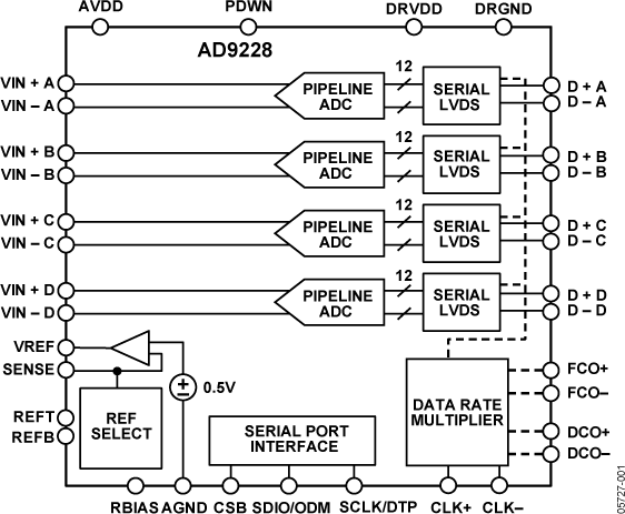
The AD9228 is a quad, 12-bit, 40/65 MSPS analog-to-digital converter (ADC) with an on-chip sample-and-hold circuit designed for low cost, low power, small size, and ease of use. The product operates at a conversion rate of up to 65 MSPS and is optimized for outstanding dynamic performance and low power in applications where a small package size is critical. The ADC requires a single 1.8 V power supply and LVPECL-/ CMOS-/LVDS-compatible sample rate clock for full performance operation. No external reference or driver components are required for many applications. The ADC automatically multiplies the sample rate clock for the appropriate LVDS serial data rate. A data clock output (DCO) for capturing data on the output and a frame clock output (FCO) for signaling a new output byte are provided. Individual channel power-down is supported and typically consumes The ADC contains several features designed to maximize flexibility and minimize system cost, such as programmable clock and data alignment and programmable digital test pattern generation. The available digital test patterns include built-in deterministic and pseudorandom patterns, along with custom user-defined test patterns entered via the serial port interface (SPI). The AD9228 is available in an RoHS compliant, 48-lead LFCSP. It is specified over the industrial temperature range of ?40?C to +85?C.PRODUCT HIGHLIGHTSSmall Footprint. Four ADCs are contained in a small, space-saving package. Low power of 119 mW/channel at 65 MSPS. Ease of Use. A data clock output (DCO) is provided that operates at frequencies of up to 390 MHz and supports double data rate (DDR) operation.User Flexibility. The SPI control offers a wide range of flexible features to meet specific system requirements. Pin-Compatible Family. This includes the AD9287 (8-bit), AD9219 (10-bit), and AD9259 (14-bit).?APPLICATIONSMedical imaging and nondestructive ultrasound Portable ultrasound and digital beam-forming systemsQuadrature radio receivers Diversity radio receivers Tape drives Optical networking Test equipment
LTC3853EUJ Demo Board | Triple, PolyPhase, 6.5V ≤ VIN ≤ 14V, VOUT1 = 1.8V/15A, VOUT2 = 1.2V/15A, VOUT3 = 2.5V/15A

Analog Devices Inc.
LTC3853EUJ Demo Board | Triple, PolyPhase, 6.5V ≤ VIN ≤ 14V, VOUT1 = 1.8V/15A, VOUT2 = 1.2V/15A, VOUT3 = 2.5V/15A
Analog Devices Inc.
Demonstration circuit 1349A is a polyphase 3-output step-down supply with tracking featuring the LTC3853EUJ. The input voltage range is 6.5V to 14V. For applications with narrow, 5V ±0.5V input range, the board has an optional resistor to tie the INTVCC pin to the VIN pin. The demo board provides three 15A outputs, with output voltages of 1.8V, 1.2V and 2.5V. The main features of the board include rail tracking, an internal 5V linear regulator for bias, RUN pins for each output, two PGOOD signals and a Mode selector that allow the converter to run in CCM, pulse skip or Burst Mode operation. Synchronization to an external clock is also possible through some minor component changes.
ADAR1000EVAL1Z

Analog Devices Inc.
ADAR1000EVAL1Z
Analog Devices Inc.
The ADAR1000 is a 4-channel, X and Ku frequency band, beamforming core chip for phased arrays. This device operates in half-duplex between receive and transmit modes. In receive mode, input signals pass through four receive channels and are combined and output at the common RF_IO pin. In transmit mode, the RF_IO input signal is split and passes through the four transmit channels. In both modes, the ADAR1000 provides a ?31 dB gain adjustment range and a full 360? phase adjustment range in each radio frequency (RF) channel, with 6-bit resolution (less than ?0.5 dB and 2.8?, respectively).A simple 4-wire serial port interface (SPI) controls all of the on-chip registers. In addition, two address pins allow SPI control of up to four devices on the same serial lines. Dedicated transmit and receive load pins also provide synchronization of all ADAR1000 chips in the same array, and a single pin controls fast switching between the transmit and receive modes. The ADAR1000 is fabricated in a silicon-germanium, bipolar CMOS (BiCMOS) process. The device is available in a compact, 88-terminal, 7 mm ? 7 mm, LGA package and is specified from ?40?C to +85?C.APPLICATIONS Phased array radar Satellite communications systems
ADP121CB-1.5-EVALZ

Analog Devices Inc.
ADP121CB-1.5-EVALZ
Analog Devices Inc.
The ADP121 is a quiescent current, low dropout, linear regulator that operates from 2.3 V to 5.5 V and provides up to 150 mA of output current. The low 135 mV dropout voltage at 150 mA load improves efficiency and allows operation over a wide input voltage range. The low 30 ?A of quiescent current at full load makes the ADP121 ideal for battery-operated portable equipment.The ADP121 is available in output voltages ranging from 1.2 V to 3.3 V. The parts are optimized for stable operation with small 1 ?F ceramic output capacitors. The ADP121 delivers good transient performance with minimal board area.Short-circuit protection and thermal overload protection circuits prevent damage in adverse conditions. The ADP121 is available in a tiny 5-lead TSOT and 4-ball 0.4 mm pitch WLCSP pack-ages and utilizes the smallest footprint solution to meet a variety of portable applications.
EVAL-AD7980SDZ

Analog Devices Inc.
EVAL-AD7980SDZ
Analog Devices Inc.
The AD7980 is a 16-bit, successive approximation, analog-to-digital converter (ADC) that operates from a single power supply, VDD. It contains a low power, high speed, 16-bit sampling ADC and a versatile serial interface port. On the CNV rising edge, it samples an analog input IN+ between 0 V to REF with respect to a ground sense IN?. The reference voltage, REF, is applied externally and can be set independent of the supply voltage, VDD. Its power scales linearly with throughput.The SPI-compatible serial interface also features the ability, using the SDI input, to daisy-chain several ADCs on a single, 3-wire bus and provides an optional busy indicator. It is compatible with 1.8 V, 2.5 V, 3 V, or 5 V logic, using the separate supply VIO.The AD7980 is housed in a 10-lead MSOP or a 10-lead QFN (LFCSP) with operation specified from ?40?C to +125?C.APPLICATIONSAutomated test equipmentData acquisition systemsMedical instrumentsMachine automation
EV-ADF4360-2EB1Z

Analog Devices Inc.
EV-ADF4360-2EB1Z
Analog Devices Inc.
The ADF4360-2 is a fully integrated integer-N synthesizerand voltage-controlled oscillator (VCO). The ADF4360-2 isdesigned for a center frequency of 2000 MHz. In addition, adivide-by-2 option is available, whereby the user gets an RFoutput of between 925 MHz and 1085 MHz.Control of all the on-chip registers is through a simple 3-wireinterface. The device operates with a power supply rangingfrom 3.0 V to 3.6 V and can be powered down when not in use.Applications Wireless handsets (DECT, GSM, PCS, DCS, WCDMA) Test equipment Wireless LANs CATV equipment
DC1410A-A

Analog Devices Inc.
DC1410A-A
Analog Devices Inc.
The LTC2498 is a 16-channel (8-differential) 24-bit No Latency ??? ADC with Easy Drive technology. The patented sampling scheme eliminates dynamic input current errors and the shortcomings of on-chip buffering through automatic cancellation of differential input current. This allows large external source impedances, and rail-to-rail input signals to be directly digitized while maintaining exceptional DC accuracy. The LTC2498 includes a high accuracy temperature sensor and an integrated oscillator. This device can be configured to measure an external signal (from combinations of 16 analog input channels operating in single ended or differential modes) or its internal temperature sensor. The integrated temperature sensor offers 1/30th ?C resolution and 2?C absolute accuracy. The LTC2498 allows a wide common mode input range (0V to VCC), independent of the reference voltage. Any combination of single-ended or differential inputs can be selected and the first conversion after a new channel is selected is valid. Access to the multiplexer output enables optional external amplifiers to be shared between all analog inputs and auto calibration continuously removes their associated offset and drift.Applications Direct Sensor Digitizer Direct Temperature Measurement Instrumentation Industrial Process Control
EVAL-AD1937AZ

Analog Devices Inc.
EVAL-AD1937AZ
Analog Devices Inc.
The AD1937 is a high performance, single-chip codec that provides four analog-to-digital converters (ADCs) with differential input and eight digital-to-analog converters (DACs) with differential output, using the Analog Devices, Inc., patented multibit sigma-delta (?-?) architecture. An I2C? port is included, allowing a microcontroller to adjust volume and many other parameters. The AD1937 operates from 3.3 V digital and analog supplies. The AD1937 is available in a 64-lead (differential output) LQFP.The AD1937 is designed for low EMI. This consideration is apparent in both the system and circuit design architectures. By using the on-board PLL to derive the master clock from the LR (frame) clock or from an external crystal, the AD1937 eliminates the need for a separate high frequency master clock and can also be used with a suppressed bit clock. The DACs and ADCs are designed using the latest Analog Devices continuous time architecture to further minimize EMI. By using 3.3 V supplies, power consumption is minimized and further reduces emissions.ApplicationsAutomotive audio systems Home theater systemsSet-top boxesDigital audio effects processorsData Sheet, Rev. 0, 9/08
LTC3855EUJ Demo Board | Dual Output, VIN = 4.5V to 25V, VOUT1 = 3.3V @ 5A, VOUT2 = 2.5V @ 5A

Analog Devices Inc.
LTC3855EUJ Demo Board | Dual Output, VIN = 4.5V to 25V, VOUT1 = 3.3V @ 5A, VOUT2 = 2.5V @ 5A
Analog Devices Inc.
Demonstration circuit 1586A is a high efficiency, dual-output (3.3V and 2.5V), synchronous buck converter with 4.5V to 25V input range. It can supply 5A maximum load current at 3.3V and 2.5V outputs. The demo board uses the LTC3855EUJ controller. The LTC3855 is a feature-rich dual-output dual-phase synchronous buck controller with on-chip drivers, remote output voltage sensing (VOUT2) and inductor DCR temperature compensation.
DC1948A
Analog Devices Inc.
DC1948A
Analog Devices Inc.
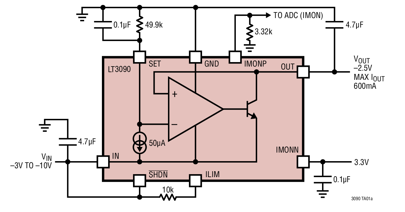
The LT3090 is a 600mA, low dropout negative linear regulator that is easily parallelable to increase output current or spread heat on surface mounted boards. Designed with a precision current reference followed by a high performance rail-to-rail voltage buffer, this regulator finds use in applications requiring precision output, high current with no heat sink, output adjustability to zero and low dropout voltage. The device can also be configured as a 3-terminal floating regulator.The LT3090 features fast transient response, high PSRR and output noise as low as 18?VRMS. The LT3090 generates a wide output voltage range (0V to ?32V) while maintaining unity gain operation. This yields virtually constant bandwidth, load regulation, PSRR and noise, regardless of the programmed output voltage.The LT3090 supplies 600mA at a typical dropout voltage of 300mV. Operating quiescent current is nominally 1mA and drops to << 1?A in shutdown. A single resistor adjusts the LT3090?s precision programmable current limit. The LT3090?s positive or negative current monitor either sources a current (0.5mA/A) or sinks a current (1mA/A) proportional to output current. Built-in protection includes reverse output protection, internal current limit with foldback and thermal shutdown with hysteresis.Applications Post Regulator for Switching Supplies Low Noise Instrumentation and RF Supplies Rugged Industrial Supplies Precision Power Supplies
