
Search results
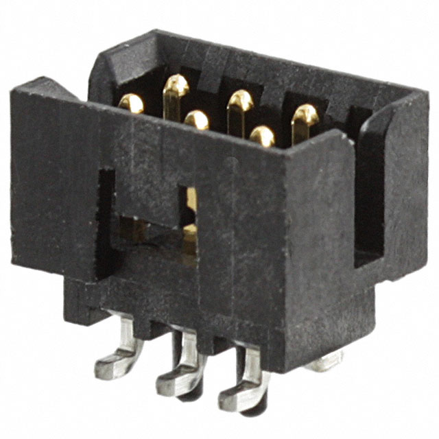
32060
Molex
Connector Header Surface Mount 6 position 0.079" (2.00mm)
| Distributor | SKU | Stock | MOQ | 1 | 10 | 50 | 100 | 1,000 | 10,000 | |
|---|---|---|---|---|---|---|---|---|---|---|
| DigiKey | WM7145DKR-ND | 2,476 | $0.78 | $0.63 | $0.63 | $0.52 | $0.70 | $0.63 | Buy |
AD7134 Evaluation Board
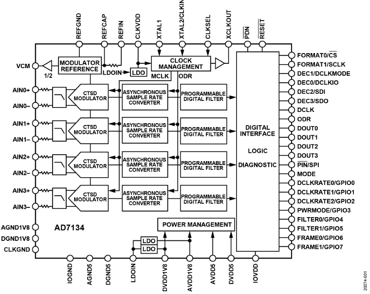
Analog Devices Inc.
AD7134 Evaluation Board
Analog Devices Inc.
The EVAL-AD7134FMCZ evaluation kit features the AD7134 24-bit, 4-channel, simultaneous sampling, 1.5 MSPS precision alias free analog-to-digital converter (ADC). Two on-board AD7134 ADCs are included to demonstrate multidevice simultaneous sampling. The EVAL-AD7134FMCZ draws power from the system demonstration platform (SDP) EVAL-SDP-CH1Z (SDP-H1) board, and the on-board dc-to-dc regulators regulate an external supply of 8 V to 14 V down to 5 V, 1.8 V, and 1.2 V to supply the AD7134 and peripheral components. Both on-board ADCs have a separate reference of 4.096 V generated by the on-board ADR444. The ADCs have three clock input options and can be clocked by a crystal input, a microelectromechanical system (MEMS) oscillator, or a complementary metal-oxide semiconductor (CMOS) clock. The EVAL-AD7134FMCZ connects to the PC USB port via the SDP-H1 board. The AD7134 evaluation software running on a PC provides full accessibility to the AD7134 device register map, as well as a data analysis interface to display key parameters and graphics from the conversion result in both time and frequency domains. For full details on the AD7134, see the AD7134 data sheet, which must be consulted in conjunction with this user guide when using the EVAL-AD7134FMCZ.
ADRF5549-EVALZ

Analog Devices Inc.
ADRF5549-EVALZ
Analog Devices Inc.
The ADRF5549 is a dual-channel, integrated, RF front-end multichip module designed for time division duplexing (TDD) applications that operates from 1.8 GHz to 2.8 GHz. The ADRF5549 is configured in dual channels with a cascading, two-stage, low noise amplifier (LNA) and a high power, silicon single-pole, double-throw (SPDT) switch.In high gain mode, the cascaded two-stage LNA and switch offer a low noise figure of 1.4 dB and a high gain of 35 dB with an output third-order intercept point (OIP3) of 32 dBm typical.In low gain mode, one stage of the two-stage LNA is in bypass mode providing 17 dB of gain at a lower current of 35 mA. In power-down mode, the LNAs are turned off, and the device draws 12 mA.In transmit operation, when RF inputs are connected to a termination pin (TERM-ChA or TERM-ChB), the switch provides a low insertion loss of 0.6 dB and handles a long-term evolution (LTE) full lifetime average (9 dB peak to average ratio (PAR)) of 40 dBm and 43 dBm for a 9 dB PAR LTE single event (ApplicationsWireless InfrastructureTDD massive multiple input and multiple output (MIMO) and active antenna systemsTDD-based communication systems
Using IBIS Models for Timing Analysis (Rev. A)

Texas Instruments
Using IBIS Models for Timing Analysis (Rev. A)
Texas Instruments
Today?s high-speed interfaces require strict timings and accurate system design. To achieve the necessary timings for a given system input/output buffer information specification (IBIS) models must be used. These models accurately represent the device drivers under various process conditions. Board characteristics such as impedance loading length number of nodes etc. affect how the device d
Universal Line Power Supply for PLC using PSR Flyback and Compact DC/DC Stages Reference Design

Texas Instruments
Universal Line Power Supply for PLC using PSR Flyback and Compact DC/DC Stages Reference Design
Texas Instruments
The PMP9185 reference design uses the UCC28710 primary-side regulated flyback controller to generate a 15V output from a univeral AC input with maximum 20W output power followied by DC/DC and LDO stages using TPS54229 and TPS650250: and 5V: 3.3V: 1.8V and 1.2V are provided. A switch on the PCB provides the freedom of supplying DC/DC and LDO from AC input or DC input.

Multicell Li-Ion and Li-Pol Battery Gas-Gauge Application Using the bqJunior
Texas Instruments
Multicell Li-Ion and Li-Pol Battery Gas-Gauge Application Using the bqJunior
Texas Instruments
The bqJunior™ series of gas gauges are designed to operate from a single-cell lithium-ion or lithium-polymer battery. Many applications that could benefit from using these gas gauges use two or more lithium cells in series where the battery voltage exceeds the operating voltage for the bqJunior™ gas gauges. This application report describes a low-component count solution for using th
Booting a TMS320C32 Target System in a C Environment
Texas Instruments
Booting a TMS320C32 Target System in a C Environment
Texas Instruments
TI supports four methods of booting a 32-bit floating point DSP following system reset. Each method uses a different combination of the TMS320C32 silicon features software and hardware tools. Each combination forms an integrated development environment that includes features to support most system boot requirements. This document describes in detail the four methods of system boot and provid
Dead-Time Generation on the TMS320C24x
Texas Instruments
Dead-Time Generation on the TMS320C24x
Texas Instruments
A Dead-Band generator protects the power semiconductors during the commutation. The dead time is programmable between 0?s and 102?s. This time range is sufficient for all kinds of power semi-conductors (MOSFET IGBT BIPOLAR and THYRISTOR) in a wide range of kW (kiloWatt) or HP (Horse Powers).TMS320C24x Dead-Band separates the transition edges of two signals: output and complemented output b
6W Boost Converter Optimized for Low Profile/Small Area

Texas Instruments
6W Boost Converter Optimized for Low Profile/Small Area
Texas Instruments
This single cell Li-Ion battery input boost converter provides a 5.3V output at 1.1A (5.8W). It achieves 90% efficiency at full load and operates at 1MHz. PMP7426 uses the TPS55340 high voltage boost converter.
TPS6501x Device Comparison (Rev. B)
Texas Instruments
TPS6501x Device Comparison (Rev. B)
Texas Instruments
This application report presents an overview on the differences among the TPS6501x family members. Devices included are the TPS65010, TPS65011, TPS65012,TPS65013, and TPS65014. It is intended to assis

| Distributor | SKU | Stock | MOQ | 1 | 10 | 50 | 100 | 1,000 | 10,000 | |
|---|---|---|---|---|---|---|---|---|---|---|
| DigiKey | 516-2121-6-ND | 206,592 | $0.50 | $0.29 | $0.29 | $0.18 | $0.13 | $0.10 | Buy |
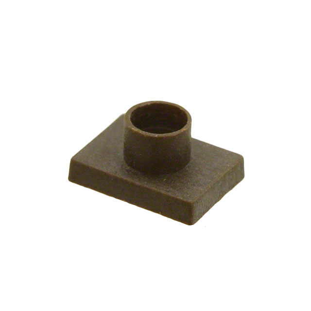
7721-10PPS
BOYD
Shoulder Washer 0.150" (3.80mm) Thick Polyphenylene Sulfide, Glass Filled
| Distributor | SKU | Stock | MOQ | 1 | 10 | 50 | 100 | 1,000 | 10,000 | |
|---|---|---|---|---|---|---|---|---|---|---|
| DigiKey | 7721-10PPSG-ND | 34,781 | 1 | $0.33 | $0.25 | $0.22 | $0.20 | $0.17 | $0.17 | Buy |
DC177A

Analog Devices Inc.
DC177A
Analog Devices Inc.
The LT1339 is a high power synchronous current mode switching regulator controller. The IC drives dual N-channel MOSFETs to create a single IC solution for high power DC/DC converters in applications up to 60V.The LT1339 incorporates programmable average current limiting, allowing accurate limiting of DC load current independent of inductor ripple current. The IC also incorporates user-adjustable slope compensation for minimization of magnetics at duty cycles up to 90%.The LT1339 timing oscillator operating frequency is programmable and can be synchronized up to 150kHz. Minimum off-time operation provides main switch protection. The IC also incorporates a soft start feature that is gated by both shutdown and undervoltage lockout conditions.An output phase reversal pin allows flexibility in configuration of converter types, including inverting and negative topologies.Applications 48V Telecom Power Supplies Personal Computers and Peripherals Distributed Power Converters Industrial Control Systems Lead-Acid Battery Backup Systems Automotive and Heavy Equipment
Altera Arria V GX FPGA Power Solution Reference Design

Texas Instruments
Altera Arria V GX FPGA Power Solution Reference Design
Texas Instruments
The PMP9449 reference design provides all the power supply rails necessary to power Altera's Arria® V GX family of FPGAs. It utilizes a TPS38600 to monitor the input supply and provide power on sequencing. This design features low cost: small footprint discrete ICs and is powered from a single 5V input.
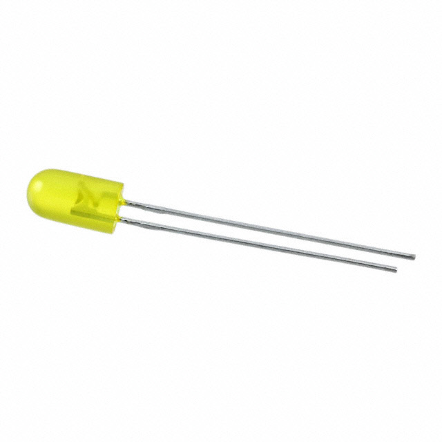
54187
Kingbright
Yellow 588nm LED Indication - Discrete 2.1V Radial
| Distributor | SKU | Stock | MOQ | 1 | 10 | 50 | 100 | 1,000 | 10,000 | |
|---|---|---|---|---|---|---|---|---|---|---|
| DigiKey | 754-1872-ND | 6,806 | $0.24 | $0.17 | $0.17 | $0.12 | $0.09 | $0.07 | Buy |

ADAM-5000/TCP
Advantech
8-slot Distributed DA&C System for Ethernet
| Distributor | SKU | Stock | MOQ | 1 | 10 | 50 | 100 | 1,000 | 10,000 | |
|---|---|---|---|---|---|---|---|---|---|---|
| DigiKey | 2084-ADAM-5000/TCP-CE-ND | 2 | 1 | $487.00 | $487.00 | $487.00 | $487.00 | $487.00 | $487.00 | Buy |
| Mouser Electronics | N/A | 0 |
LTC3634EUFD Demo Board (QFN) | VIN= 3.6V to 15V, VOUT1 =1.5V/1.8V/2.5V@±3A, VOUT2 = 0.5VIN (VTT)@±3A, VOUT3 = 0.5VIN (VTTR)@±10mA

Analog Devices Inc.
LTC3634EUFD Demo Board (QFN) | VIN= 3.6V to 15V, VOUT1 =1.5V/1.8V/2.5V@±3A, VOUT2 = 0.5VIN (VTT)@±3A, VOUT3 = 0.5VIN (VTTR)@±10mA
Analog Devices Inc.
Demonstration circuit DC1708A is a dual-output regulator focused specifically for DDR memory power applications. It is built based on the LTC3634, a high voltage dualchannel, controlled on-time monolithic synchronous buck regulator. The DC1708A has an input voltage range of 3.6V to 15V. The output voltage of the first channel, VDDQ, of the DC1708A has three fixed voltage settings: 1.5V, 1.8V and 2.5V, and is capable of delivering up to 3A of output current. The second channel, VTT, is set to regulate to half the voltage on the VDDQIN pin, which can be either the channel 1 output or an external reference voltage. It can source or sink a maximum of 3A of output current. The LTC3634 also provides a 10mA buffered output of half VDDQIN – VTTR, which is used to provide the reference voltage needed for DDR applications. With the use of a timing resistor, the DC1708A can have its operating frequency programmed from 500kHz to 4MHz. Additionally the DC1708A can be easily synchronized to an external clock, due to an internal phase-locked loop, within this same frequency range. The DC1708A VDDQ output can operate in either Burst Mode® operation or forced continuous mode. In Burst Mode operation, which is the preferred mode of low load current operation, the DC supply current is typically only 1.3mA (both channels) at no load (sleep mode), and less than 15µA in shutdown. In Burst Mode operation or continuous mode operation, the DC1708A is a very efficient circuit at high load currents: over 80% for either channel. The LTC3634 is also capable of 90° or 180° out-of-phase operation, and can allow its output to track an external voltage, either coincidentally or ratiometrically. The LTC3634 comes in a 28-pin QFN package, featuring an exposed pad on the bottom-side of the IC for better thermal performance. All of these features make the DC1708A an ideal circuit for powering DDR memory applications.