1044A
Part Number : 1044A
Analog Devices Inc.Charge Pump Switching Regulator IC Positive or Negative Fixed -Vin, 2Vin, Vin/2 1 Output 20mA 8-SOIC (0.154", 3.90mm Width)
HI3-0508A-5
Part Number : HI3-0508A-5
Analog Devices Inc.Multiplexer Switch ICs Fault Protected 8-Channel Multiplexer
LT-16
Part Number : LT-16
Analog Devices Inc.Boost Switching Regulator IC Positive Adjustable 1.263V 1 Output 1.5A (Switch) 10-TFSOP, 10-MSOP (0.118", 3.00mm Width)
LTC2496
Part Number : LTC2496
Analog Devices Inc.16 Bit Analog to Digital Converter 8, 16 Input 1 Sigma-Delta 38-QFN (5x7)

DS1646-120
Part Number : DS1646-120
Analog Devices Inc.Real Time Clock (RTC) IC Clock/Calendar 128KB Parallel 32-DIP Module (0.600", 15.24mm)

MAX5048
Part Number : MAX5048
Analog Devices Inc.Low-Side Gate Driver IC Inverting, Non-Inverting SOT-6
DS1804-010
Part Number : DS1804-010
Analog Devices Inc.Digital Potentiometer 10k Ohm 1 Circuit 100 Taps Up/Down (U/D, INC, CS) Interface 8-PDIP
MAX4289
Part Number : MAX4289
Analog Devices Inc.General Purpose Amplifier 1 Circuit Rail-to-Rail SOT-6
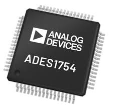
ADES1754
Part Number : ADES1754
Analog Devices Inc.14-Channel, High Voltage Data Acquisition Systems
MAX6373KA-T
Part Number : MAX6373KA-T
Analog Devices Inc.Supervisory Circuits Pin-Selectable Watchdog Timer

LTM8048MPY#PBF
Part Number : LTM8048MPY#PBF
Analog Devices Inc.Switching Voltage Regulators 3.1VIN to 32VIN Iso uModule DC/DC Conv
MAX3320AEAP+
Part Number : MAX3320AEAP+
Analog Devices Inc.RS-232 Interface IC 3-5.5V 250kbps Transceiver


DS1340Z-18
Part Number : DS1340Z-18
Analog Devices Inc.Real Time Clock (RTC) IC Clock/Calendar I2C, 2-Wire Serial 8-SOIC (0.154", 3.90mm Width)
DR45-5
Part Number : DR45-5
Analog Devices Inc.Series Voltage Reference IC Fixed 5V V ±0.04% 10 mA 8-SOIC
MAX8560EZK+
Part Number : MAX8560EZK+
Analog Devices Inc.Switching Voltage Regulators 4MHz, 500mA Synchronous Step-Down DC-DC Converters in Thin SOT and TDFN