Top Manufacturers
Stock

Displaying 4401 - 4420 of 94811

Parts from Analog Devices Inc.

MAX17059G+T10

Part Number : MAX17059G+T10

Analog Devices Inc.
The MAX17058/MAX17059 ICs are tiny fuel gauges for lithium-ion (Li+) batteries in handheld and portable equipment. The MAX17058 operates with a single Li+ cell and the MAX17059 with two Li+ cells in series.The ICs use the sophisticated Li+ battery-modeling algorithm ModelGauge™ to track the battery relative state-of-charge (SOC) continuously over a widely varying charge/discharge conditions. The ModelGauge algorithm eliminates current-sense resistor and battery-learn cycles required by other fuel gauges. Temperature compensation is implemented using the system micro-controller.On battery insertion, the ICs debounce initial voltage measurements to improve the initial SOC estimate, allowing them to be located on system side. SOC and voltage information is accessed using the I2C interface. The ICs are available in a tiny 0.9mm x 1.7mm, 8-bump wafer-level package (WLP) or a 2mm × 2mm, 8-pin TDFN package.ApplicationsDigital Still, Video, and Action CamerasHandheld Computers and TerminalsHealth and Fitness MonitorsMedical DevicesSmartphones, TabletsWireless Speakers

MAX17498BEVKIT#

Part Number : MAX17498BEVKIT#

Analog Devices Inc.
The MAX17498A/MAX17498B/MAX17498C devices are current-mode fixed-frequency flyback/boost converters with a minimum number of external components. They contain all the control circuitry required to design wide input voltage isolated and nonisolated power supplies. The MAX17498A has its rising/falling undervoltage lockout (UVLO) thresholds optimized for universal offline (85V AC to 265V AC) applications, while the MAX17498B/MAX17498C support UVLO thresholds suitable to low-voltage DC-DC applications.The switching frequency of the MAX17498A/MAX17498C is 250kHz, while that of the MAX17498B is 500kHz. These frequencies allow the use of tiny magnetic and filter components, resulting in compact, cost-effective power supplies. An EN/UVLO input allows the user to start the power supply precisely at the desired input voltage, while also functioning as an on/off pin. The OVI pin enables implementation of an input overvoltage-protection scheme that ensures that the converter shuts down when the DC input voltage exceeds the desired maximum value.The devices incorporate a flexible error amplifier and an accurate reference voltage (REF) to enable the end user to regulate both positive and negative outputs. Programmable current limit allows proper sizing and protection of the primary switching FET. The devices support a maximum duty cycle greater than 92% and provide programmable slope compensation to allow optimization of control loop performance. The devices provide an open-drain PGOOD pin that serves as a power-good indicator and enters the high-impedance state to indicate that the flyback/boost converter is in regulation. An SS pin allows programmable soft-start time for the flyback/boost converter. Hiccup-mode overcurrent protection and thermal shutdown are provided to minimize dissipation under overcurrent and overtemperature fault conditions. The devices are available in a space-saving, 16-pin (3mm x 3mm) TQFN package with 0.5mm lead spacing.ApplicationsFront-End AC/DC Power Supplies for Industrial Applications (Isolated and Nonisolated)Telecom Power SuppliesWide Input Range DC Input Flyback/Boost Industrial Power Supplies

MAX17498CATE+

Part Number : MAX17498CATE+

Analog Devices Inc.
The MAX17498A/MAX17498B/MAX17498C devices are current-mode fixed-frequency flyback/boost converters with a minimum number of external components. They contain all the control circuitry required to design wide input voltage isolated and nonisolated power supplies. The MAX17498A has its rising/falling undervoltage lockout (UVLO) thresholds optimized for universal offline (85V AC to 265V AC) applications, while the MAX17498B/MAX17498C support UVLO thresholds suitable to low-voltage DC-DC applications.The switching frequency of the MAX17498A/MAX17498C is 250kHz, while that of the MAX17498B is 500kHz. These frequencies allow the use of tiny magnetic and filter components, resulting in compact, cost-effective power supplies. An EN/UVLO input allows the user to start the power supply precisely at the desired input voltage, while also functioning as an on/off pin. The OVI pin enables implementation of an input overvoltage-protection scheme that ensures that the converter shuts down when the DC input voltage exceeds the desired maximum value.The devices incorporate a flexible error amplifier and an accurate reference voltage (REF) to enable the end user to regulate both positive and negative outputs. Programmable current limit allows proper sizing and protection of the primary switching FET. The devices support a maximum duty cycle greater than 92% and provide programmable slope compensation to allow optimization of control loop performance. The devices provide an open-drain PGOOD pin that serves as a power-good indicator and enters the high-impedance state to indicate that the flyback/boost converter is in regulation. An SS pin allows programmable soft-start time for the flyback/boost converter. Hiccup-mode overcurrent protection and thermal shutdown are provided to minimize dissipation under overcurrent and overtemperature fault conditions. The devices are available in a space-saving, 16-pin (3mm x 3mm) TQFN package with 0.5mm lead spacing.ApplicationsFront-End AC/DC Power Supplies for Industrial Applications (Isolated and Nonisolated)Telecom Power SuppliesWide Input Range DC Input Flyback/Boost Industrial Power Supplies

MAX17498CATE+T

Part Number : MAX17498CATE+T

Analog Devices Inc.
The MAX17498A/MAX17498B/MAX17498C devices are current-mode fixed-frequency flyback/boost converters with a minimum number of external components. They contain all the control circuitry required to design wide input voltage isolated and nonisolated power supplies. The MAX17498A has its rising/falling undervoltage lockout (UVLO) thresholds optimized for universal offline (85V AC to 265V AC) applications, while the MAX17498B/MAX17498C support UVLO thresholds suitable to low-voltage DC-DC applications.The switching frequency of the MAX17498A/MAX17498C is 250kHz, while that of the MAX17498B is 500kHz. These frequencies allow the use of tiny magnetic and filter components, resulting in compact, cost-effective power supplies. An EN/UVLO input allows the user to start the power supply precisely at the desired input voltage, while also functioning as an on/off pin. The OVI pin enables implementation of an input overvoltage-protection scheme that ensures that the converter shuts down when the DC input voltage exceeds the desired maximum value.The devices incorporate a flexible error amplifier and an accurate reference voltage (REF) to enable the end user to regulate both positive and negative outputs. Programmable current limit allows proper sizing and protection of the primary switching FET. The devices support a maximum duty cycle greater than 92% and provide programmable slope compensation to allow optimization of control loop performance. The devices provide an open-drain PGOOD pin that serves as a power-good indicator and enters the high-impedance state to indicate that the flyback/boost converter is in regulation. An SS pin allows programmable soft-start time for the flyback/boost converter. Hiccup-mode overcurrent protection and thermal shutdown are provided to minimize dissipation under overcurrent and overtemperature fault conditions. The devices are available in a space-saving, 16-pin (3mm x 3mm) TQFN package with 0.5mm lead spacing.ApplicationsFront-End AC/DC Power Supplies for Industrial Applications (Isolated and Nonisolated)Telecom Power SuppliesWide Input Range DC Input Flyback/Boost Industrial Power Supplies

MAX17501FATB+

Part Number : MAX17501FATB+

Analog Devices Inc.
The MAX17501 high-efficiency, high-voltage, synchronous step-down DC-DC converter with integrated MOSFETs operates over a 4.5V to 60V input voltage range. This device is offered in a fixed 3.3V , 5V or adjustable output voltage (0.9V to 92%VIN) while delivering up to 500mA of current. The output voltage is accurate to within ±1.7% over -40°C to +125°C. The MAX17501 is available in a compact TDFN package. Simulation models are available.The device features peak-current-mode control with pulse-width modulation (PWM). Users can choose devices with either pulse frequency modulation (PFM) or forced PWM scheme. PFM devices skip pulses at light load for higher efficiency, while forced-PWM devices operate with fixed switching frequency at any load for noise sensitive-applications. The low-resistance, on-chip MOSFETs ensure high efficiency at full load and simplify the layout.A programmable soft-start feature allows users to reduce input inrush current. The device also incorporates an output enable/undervoltage lockout pin (EN/UVLO) that allows the user to turn on the part at the desired input-voltage level. An open-drain active-low RESET pin provides a delayed power-good signal to the system upon achieving successful regulation of the output voltage.ApplicationsBase Station, VOIP, TelecomBattery-Powered EquipmentGeneral-Purpose Point-of-LoadHome TheaterHVAC and Building ControlIndustrial Process Control

MAX17502FTEVKIT#

Part Number : MAX17502FTEVKIT#

Analog Devices Inc.
Create a design and simulate using EE-Sim®: MAX17502The MAX17502 high-efficiency, high-voltage, synchronous step-down DC-DC converter with integrated MOSFETs operates over a 4.5V to 60V input voltage range. This device is offered in a fixed 3.3V, 5V, or adjustable output voltage (0.9V to 92%VIN) while delivering up to 1A of current. The output voltage is accurate to within ±1.7% over -40°C to +125°C. The MAX17502 is available in compact TDFN and TSSOP packages. Simulation models are available.The device features peak-current-mode control with pulse-width modulation (PWM) and operates with fixed switching frequency at any load. The low-resistance, on-chip MOSFETs ensure high efficiency at full load and simplify the layout.A programmable soft-start feature allows users to reduce input inrush current. The device also incorporates an output enable/undervoltage lockout pin (EN/UVLO) that allows the user to turn on the part at the desired input-voltage level. An open-drain active-low RESET pin provides a delayed power-good signal to the system upon achieving successful regulation of the output voltage.ApplicationsBase Station, VOIP, TelecomBattery-Powered EquipmentGeneral-Purpose Point-of-LoadHome TheaterHVAC and Building ControlIndustrial Process Control

MAX17502GATB+T

Part Number : MAX17502GATB+T

Analog Devices Inc.
Create a design and simulate using EE-Sim®: MAX17502The MAX17502 high-efficiency, high-voltage, synchronous step-down DC-DC converter with integrated MOSFETs operates over a 4.5V to 60V input voltage range. This device is offered in a fixed 3.3V, 5V, or adjustable output voltage (0.9V to 92%VIN) while delivering up to 1A of current. The output voltage is accurate to within ±1.7% over -40°C to +125°C. The MAX17502 is available in compact TDFN and TSSOP packages. Simulation models are available.The device features peak-current-mode control with pulse-width modulation (PWM) and operates with fixed switching frequency at any load. The low-resistance, on-chip MOSFETs ensure high efficiency at full load and simplify the layout.A programmable soft-start feature allows users to reduce input inrush current. The device also incorporates an output enable/undervoltage lockout pin (EN/UVLO) that allows the user to turn on the part at the desired input-voltage level. An open-drain active-low RESET pin provides a delayed power-good signal to the system upon achieving successful regulation of the output voltage.ApplicationsBase Station, VOIP, TelecomBattery-Powered EquipmentGeneral-Purpose Point-of-LoadHome TheaterHVAC and Building ControlIndustrial Process Control

MAX17503SATP+

Part Number : MAX17503SATP+

Analog Devices Inc.
The Himalaya series of voltage regulator ICs, power modules, and chargers enable cooler, smaller, and simpler power supply solutions. The MAX17503/MAX17503S high-efficiency, high-voltage, synchronously rectified step-down converter with dual integrated MOSFETs operates over a 4.5V to 60V input. It delivers up to 2.5A and 0.9V to 90%VIN output voltage. Built-in compensation across the output voltage range eliminates the need for external components. The feedback (FB) regulation accuracy over -40°C to +125°C is ±1.1%. The device is available in a compact (4mm x 4mm) TQFN-EP lead(Pb)-free package with an exposed pad. Simulation models are available.The device features a peak-current-mode control architecture with a MODE feature that can be used to operate the device in pulse-width modulation (PWM), pulse-frequency modulation (PFM), or discontinuous-conduction mode (DCM) control schemes. PWM operation provides constant frequency operation at all loads, and is useful in applications sensitive to switching frequency. PFM operation disables negative inductor current and additionally skips pulses at light loads for high efficiency. DCM features constant frequency operation down to lighter loads than PFM mode, by not skipping pulses, but only disabling negative inductor current at light loads. DCM operation offers efficiency performance that lies between PWM and PFM modes.The MAX17503S offersa lower minimum on-time that allows for higher switchingfrequencies and a smaller solution size.A programmable soft-start feature allows users to reduce input inrush current. The device also incorporates an output enable/input undervoltage lockout pin (EN/UVLO) that allows the user to turn on the part at the desired input-voltage level. An open-drain active-low RESET pin provides a delayed power-good signal to the system upon achieving successful regulation of the output voltage.ApplicationsBase Station Power SuppliesDistributed Supply RegulationGeneral-Purpose Point-of-LoadHigh-Voltage Single-Board SystemsIndustrial Power SuppliesWall Transformer Regulation

MAX17503SATP+T

Part Number : MAX17503SATP+T

Analog Devices Inc.
The Himalaya series of voltage regulator ICs, power modules, and chargers enable cooler, smaller, and simpler power supply solutions. The MAX17503/MAX17503S high-efficiency, high-voltage, synchronously rectified step-down converter with dual integrated MOSFETs operates over a 4.5V to 60V input. It delivers up to 2.5A and 0.9V to 90%VIN output voltage. Built-in compensation across the output voltage range eliminates the need for external components. The feedback (FB) regulation accuracy over -40°C to +125°C is ±1.1%. The device is available in a compact (4mm x 4mm) TQFN-EP lead(Pb)-free package with an exposed pad. Simulation models are available.The device features a peak-current-mode control architecture with a MODE feature that can be used to operate the device in pulse-width modulation (PWM), pulse-frequency modulation (PFM), or discontinuous-conduction mode (DCM) control schemes. PWM operation provides constant frequency operation at all loads, and is useful in applications sensitive to switching frequency. PFM operation disables negative inductor current and additionally skips pulses at light loads for high efficiency. DCM features constant frequency operation down to lighter loads than PFM mode, by not skipping pulses, but only disabling negative inductor current at light loads. DCM operation offers efficiency performance that lies between PWM and PFM modes.The MAX17503S offersa lower minimum on-time that allows for higher switchingfrequencies and a smaller solution size.A programmable soft-start feature allows users to reduce input inrush current. The device also incorporates an output enable/input undervoltage lockout pin (EN/UVLO) that allows the user to turn on the part at the desired input-voltage level. An open-drain active-low RESET pin provides a delayed power-good signal to the system upon achieving successful regulation of the output voltage.ApplicationsBase Station Power SuppliesDistributed Supply RegulationGeneral-Purpose Point-of-LoadHigh-Voltage Single-Board SystemsIndustrial Power SuppliesWall Transformer Regulation

MAX17515ELI+

Part Number : MAX17515ELI+

Analog Devices Inc.
The MAX17515 is a fixed-frequency, step-down power module in a thermally efficient system-in-package (SiP) package that operates from a 2.4V to 5.5V input supply voltage and supports output currents up to 5A. The device includes switch-mode power-supply controller, dual n-channel MOSFET power switches, a fully shielded inductor, as well as compensation components. The device supports 0.75V to 3.6V programmable output voltage. The high level of integration significantly reduces design complexity, manufacturing risks, and offers a true “plug-and-play” power-supply solution, reducing the time to market.The device operates at a fixed 1MHz that requires smaller input and output capacitor size. The internal fixed constant gain at the error-amplifier output results in output-voltage positioning with respect to the load current. The fixed internal digital soft-start limits the input inrush current at startup. The device also operates in pulse-skipping mode at light loads to improve the light-load efficiency.The MAX17515 is available in a thermally enhanced, compact 28-pin, 10mm × 6.5mm x 2.8mm SiP package and can operate over the -40°C to +85°C industrial temperature range.ApplicationsATE EquipmentBase Station Point-of-Load RegulatorFPGA and DSP Point-of-Load RegulatorIndustrial Control EquipmentMedical EquipmentServers

MAX17595ATE+T

Part Number : MAX17595ATE+T

Analog Devices Inc.
The MAX17595/MAX17596/MAX17597 is a family of peak-current-mode controllers for design of wide input-voltage flyback and boost regulators. The MAX17595 offers optimized input thresholds for universal input AC-DC converters and telecom DC-DC (36V to 72V input range) power supplies. The MAX17596/MAX17597 offer input thresholds suitable for low-voltage DC-DC applications (4.5V to 36V). The MAX17597 implements a boost converter. All three controllers contain a built-in gate driver for external n-channel MOSFETs.The MAX17595/MAX17596/MAX17597 house an internal error amplifier with 1% accurate reference, eliminating the need for an external reference. The switching frequency is programmable from 100kHz to 1MHz with an accuracy of 8%, allowing optimization of magnetic and filter components, resulting in compact and cost-effective power conversion. For EMI-sensitive applications, the MAX17595/MAX17596/MAX17597 family incorporates a programmable frequency dithering scheme, enabling low-EMI spread-spectrum operation.Users can start the power supply precisely at the desired input voltage, implement input overvoltage protection, and program soft-start time. A programmable slope compensation scheme is provided to ensuree stability of the peak-current-mode control scheme.Hiccup-mode overcurrent protection and thermal shutdown are provided to minimize dissipation in overcurrent and overtemperature fault conditions.ApplicationsBattery-Powered ApplicationsIndustrial and Telecom ApplicationsUniversal Input Offline AC-DC Power SuppliesWide-Range DC-Input Flyback/Boost Battery Chargers

MAX17596EVKIT#

Part Number : MAX17596EVKIT#

Analog Devices Inc.
The MAX17595/MAX17596/MAX17597 is a family of peak-current-mode controllers for design of wide input-voltage flyback and boost regulators. The MAX17595 offers optimized input thresholds for universal input AC-DC converters and telecom DC-DC (36V to 72V input range) power supplies. The MAX17596/MAX17597 offer input thresholds suitable for low-voltage DC-DC applications (4.5V to 36V). The MAX17597 implements a boost converter. All three controllers contain a built-in gate driver for external n-channel MOSFETs.The MAX17595/MAX17596/MAX17597 house an internal error amplifier with 1% accurate reference, eliminating the need for an external reference. The switching frequency is programmable from 100kHz to 1MHz with an accuracy of 8%, allowing optimization of magnetic and filter components, resulting in compact and cost-effective power conversion. For EMI-sensitive applications, the MAX17595/MAX17596/MAX17597 family incorporates a programmable frequency dithering scheme, enabling low-EMI spread-spectrum operation.Users can start the power supply precisely at the desired input voltage, implement input overvoltage protection, and program soft-start time. A programmable slope compensation scheme is provided to ensuree stability of the peak-current-mode control scheme.Hiccup-mode overcurrent protection and thermal shutdown are provided to minimize dissipation in overcurrent and overtemperature fault conditions.ApplicationsBattery-Powered ApplicationsIndustrial and Telecom ApplicationsUniversal Input Offline AC-DC Power SuppliesWide-Range DC-Input Flyback/Boost Battery Chargers

MAX17599ATE+T

Part Number : MAX17599ATE+T

Analog Devices Inc.
The MAX17598/MAX17599 low IQ, active clamp current-mode PWM controllers contain all the control circuitry required for the design of wide-input isolated/non-isolated forward-converter industrial power supplies. The MAX17598 is well-suited for universal input (rectified 85V AC to 265V AC) or telecom (36V DC to 72V DC) power supplies. The MAX17599 is optimized for low-voltage industrial supplies (4.5V DC to 36V DC).The devices include an AUX driver that drives an auxiliary MOSFET (clamp switch) that helps implement the active-clamp transformer reset topology for forward converters. Such a reset topology has several advantages including reduced voltage stress on the switches, transformer size reduction due to larger allowable flux swing, and improved efficiency due to elimination of dissipative snubber circuitry. Programmable dead time between the AUX and main driver allows for zero voltage switching (ZVS).The switching frequency is programmable from 100kHz to 1MHz for the devices with an accuracy of ±8% using an external resistor. This allows optimization of the magnetic and filter components, resulting in compact, cost-effective isolated/nonisolated power supplies. For EMI-sensitive applications, the ICs incorporate a programmable frequency-dithering scheme, enabling low-EMI spread-spectrum operation.An input undervoltage lockout (EN/UVLO) is provided for programming input-supply start voltage, and to ensure proper operation during brownout conditions. EN/UVLO input is also used to turn on/off the ICs. Input overvoltage (OVI) protection scheme is provided to make sure that the regulator shuts down when input supply exceeds its maximum allowed value.To control inrush current, the devices incorporate an SS pin to set the soft-start time for the regulators. Power dissipation under fault conditions is minimized by hiccup overcurrent protection (hiccup mode). Soft-stop feature provides safe discharging of the clamp capacitor when the device is turned off, and allows the controller to restart in a well-controlled manner. Additionally, negative current limit is provided in the current-sense circuitry, helping limit clamp switch current under dynamic operating conditions.SYNC feature is provided to synchronize multiple converters to a common external clock in noise-sensitive applications. Overtemperature fault triggers thermal shutdown for reliable protection of the device. The ICs are available in a 16-pin, TQFN package with 0.5 mm lead spacing.ApplicationsIndustrial Power SuppliesIsolated Battery ChargersServers and Embedded ComputingTelecom and Datacom Power Supplies

ADG5212BRUZ

Part Number : ADG5212BRUZ

Analog Devices Inc.
The ADG5212 / ADG5213 contain four independent single-pole/single-throw (SPST) switches. The ADG5212 switches turn on with Logic 1. The ADG5213 has two switches with digital control logic similar to that of the ADG5212; however, the logic is inverted on the other two switches. Each switch conducts equally well in both directions when on, and each switch has an input signal range that extends to the supplies. In the off condition, signal levels up to the supplies are blocked.The ADG5212 and ADG5213 do not have a VL pin. The digital inputs are compatible with 3 V logic inputs over the full operating supply range. The ultralow capacitance and charge injection of these switches make them ideal solutions for data acquisition and sample-and-hold applications, where low glitch and fast settling are required. Fast switching speed together with high signal bandwidth make the parts suitable for video signal switching.APPLICATIONS Automatic test equipment Data acquisition Instrumentation Avionics Audio and video switching Communication systemsPRODUCT HIGHLIGHTS Trench Isolation Guards Against Latch-Up. A dielectric trench separates the P and N channel transistors thereby preventing latch-up even under severe overvoltage conditions. Ultralow capacitance and < 1 pC charge injection. Dual-Supply Operation. For applications where the analog signal is bipolar, the ADG5212 / ADG5213 can be operated from dual supplies up to ±22 V. Single-Supply Operation. For applications where the analog signal is unipolar, the ADG5212 / ADG5213 can be operated from a single rail power supply up to 40 V. 3 V Logic Compatible Digital Inputs. VINH = 2.0 V, VINL = 0.8 V. No VL Logic Power Supply Required.

ADG5234BCPZ-RL7

Part Number : ADG5234BCPZ-RL7

Analog Devices Inc.
The ADG5233 and ADG5234 are monolithic industrial CMOS analog switches comprising three independently selectable single-pole, double throw (SPDT) switches and four independently selectable SPDT switches, respectively.All channels exhibit break-before-make switching action that prevents momentary shorting when switching channels. An EN input on the ADG5233 (LFCSP and TSSOP packages) is used to enable or disable the device. When disabled, all channels are switched off.The ultralow capacitance and charge injection of these switches make them ideal solutions for data acquisition and sample-and-hold applications, where low glitch and fast settling are required. Fast switching speed coupled with high signal bandwidth make these devices suitable for video signal switching.APPLICATIONS Automatic test equipment Data acquisition Instrumentation Avionics Audio and video switching Communication systemsPRODUCT HIGHLIGHTS Trench Isolation Guards Against Latch-Up. A dielectric trench separates the P and N channel transistors thereby preventing latch-up even under severe overvoltage conditions. Ultralow Capacitance and −0.6 pC Charge Injection. Dual-Supply Operation. For applications where the analog signal is bipolar, the ADG5233/ADG5234 can be operated from dual supplies up to ±22 V. Single-Supply Operation. For applications where the analog signal is unipolar, the ADG5233/ADG5234 can be operated from a single-rail power supply up to 40 V. 3 V Logic-Compatible Digital Inputs. VINH = 2.0 V, VINL = 0.8 V. No VL Logic Power Supply Required.

ADG5421BRMZ-RL7

Part Number : ADG5421BRMZ-RL7

Analog Devices Inc.
The ADG5421 is a monolithic industrial CMOS analog switch containing two independent latch-up immune single-pole/single-throw (SPST) switches. Each switch conducts equally well in both directions when on, and has an input signal range that extends to the power supplies. In the off condition, signal levels up to the supplies are blocked. Both ADG5421 switches are turned on with a Logic 1 input. The ADG5423 exhibits break-before-make action for use in multiplexer applications.The ultralow on resistance and on-resistance flatness of these switches make them ideal solutions for data acquisition and gain switching applications, where low distortion is critical. The latch-up immune construction, and high ESD rating, makes these switches more robust in harsh environments.PRODUCT HIGHLIGHTS Trench isolation guards against latch-up. A dielectric trench separates the P and N channel transistors thereby preventing latch-up even under severe overvoltage conditions. Low RON. Dual-supply operation. For applications where the analog signal is bipolar, the ADG5421 can be operated from dual supplies up to ±22 V. Single-supply operation. For applications where the analog signal is unipolar, the ADG5421 can be operated from a single-rail power supply up to 40 V. 3 V logic compatible digital inputs: VINH = 2.0 V, VINL = 0.8 V. No VL logic power supply required. Available in 10-lead MSOP package. APPLICATIONS High voltage signal routing Automatic test equipment Analog front-end circuits Precision data acquisition Industrial Instrumentation Amplifier gain select Relay replacement

ADL5363ACPZ-R7

Part Number : ADL5363ACPZ-R7

Analog Devices Inc.
The ADL5363 uses a highly linear, doubly balanced passive mixer core along with integrated RF and local oscillator (LO) balancing circuitry to allow for single-ended operation. The ADL5363 incorporates an RF balun to provide optimal performance over a 2300 MHz to 2900 MHz input frequency range. The balanced passive mixer arrangement provides good LO-to-RF leakage, typically better than −30 dBm, and excellent intermodulation performance. The balanced mixer core also provides extremely high input linearity, allowing the device to be used in demanding cellular applications where in-band blocking signals might otherwise result in the degradation of dynamic performance.The ADL5363 provides two switched LO paths that can be used in TDD applications where it is desirable to rapidly switch between two local oscillators. LO current can be externally set using a resistor to minimize dc current commensurate with the desired level of performance. For low voltage applications, the ADL5363 is capable of operation at voltages down to 3.3 V with substantially reduced current. For low voltage operation, an additional logic pin is provided to power down (

ADL5506-EVALZ

Part Number : ADL5506-EVALZ

Analog Devices Inc.
The ADL5506 is a complete, low cost subsystem for the measurement of RF signals in the 30 MHz to 4.5 GHz frequency range, with a typical dynamic range of 45 dB, intended for use in a wide variety of wireless terminal devices. It provides a wider dynamic range and better accuracy than is possible using discrete diode detectors. In particular, its temperature stability is excellent over −40°C to +85°C.Its high sensitivity allows measurement of low power levels, thus reducing the amount of power that needs to be coupled to the detector. It is essentially a voltage responding device, with a typical dynamic range of 45 dB.For convenience, the signal is internally ac-coupled, using a 5 pF capacitor and a broadband 50 Ω match, with an external shunt resistor of 52 Ω. This high-pass coupling, with a corner at approximately 19 MHz, determines the lowest operating frequency. Therefore, the source can be dc grounded.The ADL5506 output increases from approximately 0.14 V to a little over 1 V as the input signal level increases from 1.25 mV rms (−45 dBm) to 224 mV rms (0 dBm). The output is proportional to the logarithm of the input power level; that is, the reading is presented directly in decibels and is scaled about 18 mV/dB at 900 MHz. A capacitor can be connected between the VLOG pin and the CFLT pin when it is desirable to increase the time interval over which averaging of the input waveform occurs.The ADL5506 is available in a 6-ball WLCSP and consumes 3.8 mA from a 3.0 V supply. When powered down, the typical disable supply current is

ADL5611-EVALZ

Part Number : ADL5611-EVALZ

Analog Devices Inc.
The ADL5611 is a single-ended RF/IF gain block amplifier that provides broadband operation from 30 MHz to 6 GHz. The ADL5611 provides a low noise figure of 2.1 dB with a very high OIP3 of 40.0 dBm simultaneously, which delivers a high dynamic range.The ADL5611 provides a gain of 22.2 dB that is stable over frequency, temperature, and power supply, and from device to device. The amplifier is offered in the industry-standard SOT-89 package and is internally matched to 50 Ω at the input and output, making the ADL5611 easy to implement in a wide variety of applications. The only external parts required are the input and output ac coupling capacitors, power supply decoupling capacitors, and bias inductor.The ADL5611 has a high ESD rating of ±1.5 kV (Class 1C) and is fully specified for operation across a wide temperature range of −40°C to +105°C. A fully populated RoHS-compliant evaluation board is available.

ADM1075-1ACPZ-RL7

Part Number : ADM1075-1ACPZ-RL7

Analog Devices Inc.
The ADM1075 is a full feature, negative voltage, hot swap controllerwith constant power foldback and high accuracy digital currentand voltage measurement that allows boards to be safely insertedand removed from a live -48 V backplane. The part providesprecise and robust current limiting and protection against bothtransient and nontransient short circuits and overvoltage andundervoltage conditions. The ADM1075 typically operates froma negative voltage of -35 V to -80 V and, due to shunt regulation,has excellent voltage transient immunity. The operating range ofthe part is flexible due to the shunt regulator, and the part can bepowered directly by a 10 V rail to save shunt power dissipation(see the Powering the ADM1075 section for more details).A full-scale current limit of 25 mV or 50 mV can be selected bychoosing the appropriate model. The maximum current limit isset by the combination of the sense resistor, RSENSE, and the inputvoltage on the ISET pin, using external resistors. This allows finetuning of the trip voltage so that standard sense resistors can beused. Inrush current is limited to this programmable value bycontrolling the gate drive of an external N-channel FET. A builtinsoft start function allows control of the inrush current profile byan external capacitor on the soft start (SS) pin.Refer to the datasheet for more information.PRODUCT HIGHLIGHTS Constant Power Foldback. Maximum FET power set by a PLIM resistor divider. This eases complexity when designing to maintain FET SOA. Adjustable Current Limit. The current limit is adjustable via the ISET pin allowing for the use of a standard value sense resistor. 12-Bit ADC. Accurate voltage, current, and power measurements. Also enables calculation of energy consumption over time. PMBus Interface. PMBus fast mode compliant interface used to read back status and data registers and set warning and fault limits. Fault Recording. Latched status registers provide useful debugging information to help trace faults in high reliability systems. Built-In Soft Start. Soft start capacitor controls inrush current profile with di/dt control.APPLICATIONS Telecommunication and data communication equipment Central office switching -48 V distributed power systems Negative power supply control High availability servers

Displaying 4401 - 4420 of 94811

Latest Parts

IN STOCK 13664
Buy

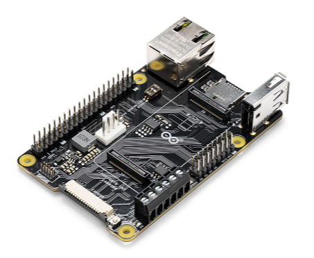
ASX00049

Arduino

* $43.59 - * $50.60

IN STOCK 2855
Buy

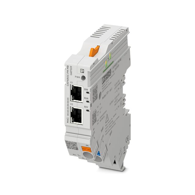
1687559

Phoenix Contact Ltd

[no prices available]

IN STOCK 2
Buy

Reference Designs

RD006

Wurth Elektronik

RD006 - 3 W Dual-output isolated auxiliary supply for communication interfaces and measurement systems

CN0583

Analog Devices Inc.

Multistandard Micropower Verified Smoke Detection System-on-Module

Technical Resources

EVALUATION KITS

EVAL-AD7124-8SDZ

Analog Devices Inc.

$0.00 - * $82.07

IN STOCK 792
Buy
View All