ADRF6821ACPZ
Part Number : ADRF6821ACPZ
Analog Devices Inc.Wideband DPD Receiver ;RoHS Compliant: Yes
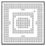
ADSP-SC583CBCZ-4A
Part Number : ADSP-SC583CBCZ-4A
Analog Devices Inc.ARM 2x 3Mb SHARC single DDR LPC packa
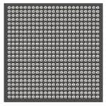
ADSP-SC587BBCZ-4B
Part Number : ADSP-SC587BBCZ-4B
Analog Devices Inc.ARM 2xSHARC dual DDR HPC package
ADUCM362BCPZ128RL7
Part Number : ADUCM362BCPZ128RL7
Analog Devices Inc.Cortex M3 + 16K/128K + Dual 24bit SD AFE
ADUM142E1WBRQZ-RL7
Part Number : ADUM142E1WBRQZ-RL7
Analog Devices Inc.Robust Quad Channel Isolator W/ Output
ADUM221N0WBRWZ-RL
Part Number : ADUM221N0WBRWZ-RL
Analog Devices Inc.IC Robust Auto Dual ISO 2:1 Channel
ADUM4120CRIZ
Part Number : ADUM4120CRIZ
Analog Devices Inc.Iso Gate Drvr w/2A output w/Glitch Filtr ;RoHS Compliant: Yes
ADUM4121-1BRIZ-RL
Part Number : ADUM4121-1BRIZ-RL
Analog Devices Inc.Iso Gate Drvr w/Miller clamp w/o TSD
ADUM4121ARIZ
Part Number : ADUM4121ARIZ
Analog Devices Inc.Iso Gate Drvr w/Miller clamp w/TSD ;RoHS Compliant: Yes
ADUM4121CRIZ-RL
Part Number : ADUM4121CRIZ-RL
Analog Devices Inc.Iso Gate Drvr w/Miller clamp w/TSD
AD6688BBPZ-3000
Part Number : AD6688BBPZ-3000
Analog Devices Inc.RF Diversity & 1.2GHz BW Observation Rec


