ADG5249FBCPZ-RL7
Part Number : ADG5249FBCPZ-RL7
Analog Devices Inc.55V OV Detect +5V 25V Dual 4:1Mux
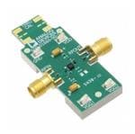
ADG904SCPZ-EP-RL7
Part Number : ADG904SCPZ-EP-RL7
Analog Devices Inc.1GHz SPST Sw. (50 Ohm Termination) I.C.
ADM3065EARMZ
Part Number : ADM3065EARMZ
Analog Devices Inc.3->5V 50Mbps RS-485/RS-422 Transceiver ;RoHS Compliant: Yes
ADM8316WDW49ARJZR7
Part Number : ADM8316WDW49ARJZR7
Analog Devices Inc.WD MRb PPb 30msTO 102msWD 4.9V
ADN4652BRSZ-RL7
Part Number : ADN4652BRSZ-RL7
Analog Devices Inc.3.75kVrms LVDS Iso 600Mbps Dual Rx & Tx
ADPD2214ACPZ-RL
Part Number : ADPD2214ACPZ-RL
Analog Devices Inc.Ultra-Low Noise Integr Intensity Sensor
ADP7183ACPZN0.5-R7
Part Number : ADP7183ACPZN0.5-R7
Analog Devices Inc.Ultra Low Noise High PSRR #Negative LDO
ADP7183ACPZN1.5-R7
Part Number : ADP7183ACPZN1.5-R7
Analog Devices Inc.Ultra Low Noise High PSRR #Negative LDO
ADP7183ACPZN2.5-R7
Part Number : ADP7183ACPZN2.5-R7
Analog Devices Inc.Ultra Low Noise High PSRR #Negative LDO
ADRF5021BCCZN-R7
Part Number : ADRF5021BCCZN-R7
Analog Devices Inc.High isolation SPDT 30GHz low cut-off


