
LTC1682CMS8 | Doubler Charge Pump with Linear Regulator, Adjustable, 1.8 to 4.4VIN, 2.5 to 5.5VOUT @ 50mA
Analog Devices Inc.DC249A-A: Demo Board for the LTC1682 Doubler Charge Pumps with Low Noise Linear Regulator.
LTC1682CMS8-5 | Doubler Charge Pump with Linear Regulator, Fixed, 2.7 to 4.4VIN, 5.0VOUT @ 50mA
Analog Devices Inc.DC249A-B: Demo Board for the LTC1682 Doubler Charge Pumps with Low Noise Linear Regulator.

LTM8002 40VIN, 2.5A Step-Down µModule Regulator
Analog Devices Inc.Demonstration circuit 2501A features the LTM®8002, a 40V, 2.5A step-down µModule® regulator. This demo circuit is configured to deliver a 5.0V output from an input
voltage between 6.0V to 40V at a switching frequency of 1MHz. The wide input range of the LTM8002 allows a variety of input sources such as automotive batteries and industrial supplies. Under light load conditions, the available Burst Mode® operation supports high efficiency with low output ripple.
The demo board has an EMI filter installed. The EMI performance of the board is shown in Figure 6 and Figure 7.
The LTM8002 data sheet gives complete description of the device, operation and application information. The data sheet must be read in conjunction with this demo manual prior to working on or modifying demo circuit 2501A.

DC2504A
Analog Devices Inc.The LT8630 is a current mode PWM step-down DC/DC converter with internal synchronous switches that provide current for output loads up to 0.6A. The wide input range of 3V to 100V makes the LT8630 suitable for regulating power from a wide variety of sources, including automotive and industrial systems and 36V to 72V telecom supplies. Variable frequency boundary mode switching maximizes efficiency across a wide range of input voltages. Low ripple Burst Mode operation enables high efficiency operation down to very low output currents while keeping the output ripple below 5mV. The soft-start feature controls the ramp rate of the output voltage, eliminating input current surge during start-up, while also providing output tracking. A power good flag signals when the output voltage is within ?7.5% of the regulated output. Undervoltage lockout can be programmed using the EN/UV pin. Shutdown mode reduces the total quiescent current to < 5?A. The LT8630 is available in a 20-lead TSSOP package with exposed pad for low thermal resistance and high voltage lead spacing.APPLICATIONS Automotive Supplies Telecom Supplies Distributed Supply Regulation

LTC1503CMS8-2 | High Efficiency Inductorless Step-Down DC/DC Converter, 2.4 to 6VIN, 2VOUT @ 100mA
Analog Devices Inc.DC250A-A: Demo Board for the LTC1503 High Efficiency Inductorless Step-Down DC/DC Converter.

LTC2975 Demo Board: ±12V, ±48V Power Supply Management [requires DC1613]
Analog Devices Inc.The DC2518A is a demonstration system for the LTC2975 Power System Manager that interfaces to various regulators. The board contains all the circuitry needed to use the LTC2975 in a power system and control four power supplies. The four power supplies include linear and switching regulators for the purpose of demonstrating a variety of methods to sense voltage and current. The demo board provides a sophisticated, digitally programmable 4-channel power supply system.

DC2527A-B
Analog Devices Inc.The LTM4646 is a complete dual 10A output switching mode DC/DC power supply. Included in the package are the switching controller, power FETs, inductors, and all supporting components. Operating from an input voltage range of 4.5V to 20V, the LTM4646 supports two outputs each with an output voltage range of 0.6V to 5.5V, set by external resistors. Its high efficiency design delivers up to 10A continuous current for each output. Only a few input and output capacitors are needed.The device supports frequency synchronization, multiphase operation, high efficiency light load operation and output voltage tracking for supply rail sequencing and has an on-board temperature diode per channel for device temperature monitoring. High switching frequency and a current mode architecture enable a very fast transient response to line and load changes without sacrificing stability.Fault protection features include overvoltage and overcurrent protection. The power module is offered in a small footprint 11.25mm ? 15mm ? 5.01mm BGA package. The LTM4646 is available with SnPb or RoHS compliant terminal finish.Applications Point-of-Load Power Supplies Telecom and Networking Equipment Industrial Equipment Medical Equipment

LTC7810ELXE High Input Voltage Dual Output Synchronous Buck Converter
Analog Devices Inc.Demonstration circuit 2529A is a dual output synchronous buck converter featuring the LTC7810ELXE in a 48-lead eLQFP package.
Key features of this board include: an optional on-board NMOS LDO for DRVCC; jumper for spread-spectrum option; optional resistors for single output dual phase operation; a mode selector that allows the converter to run in CCM, pulse-skipping, adjustable burst clamp or default Burst Mode® operation; SYNC turret for Poly-Phase® operation.
The input voltage range of this demo board is from 16V to 130V and it uses a sense resistor for overcurrent protection. The LTC7810 data sheet gives a complete description of the part, operation and application information and must be read in conjunction with this demo manual for DC2529A.
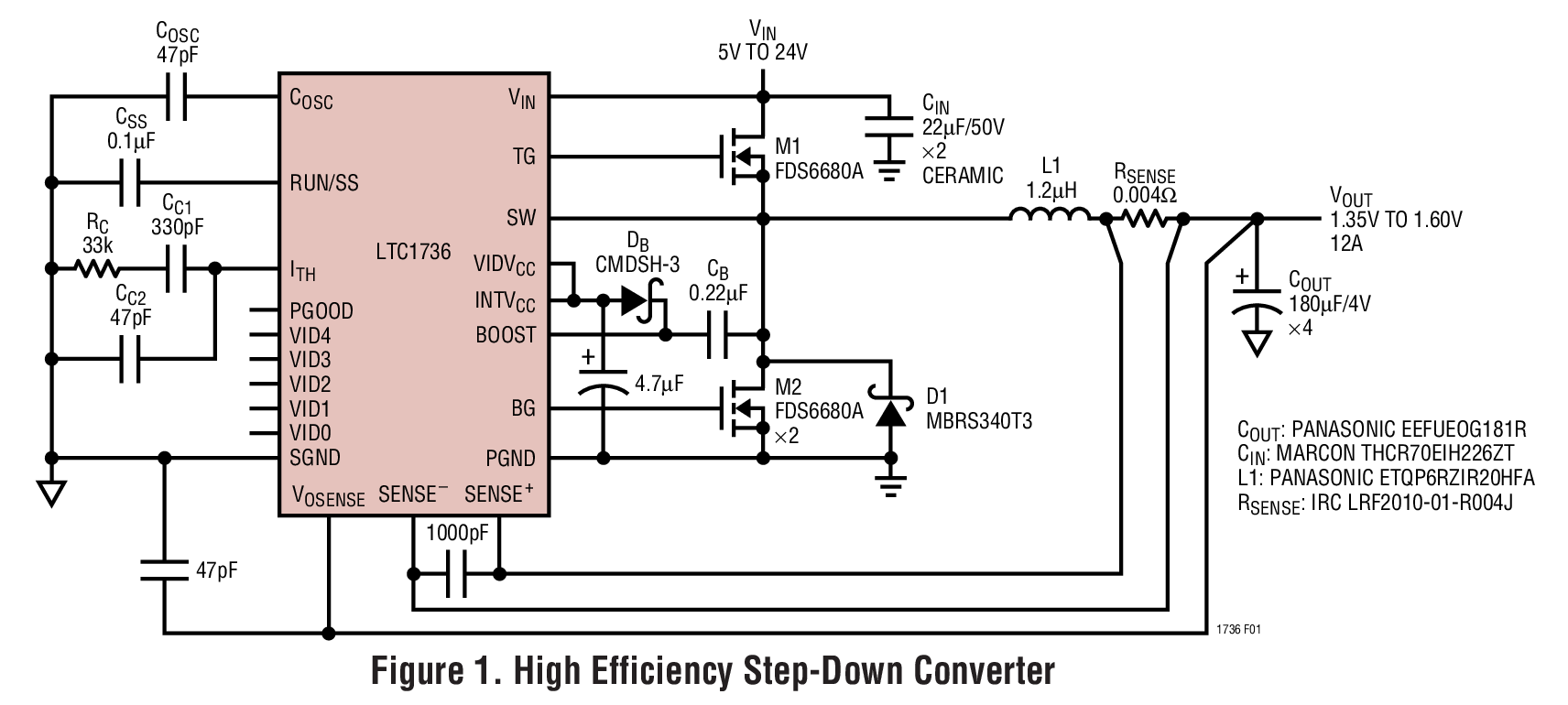
LTC1736CG | 5 Bit, VID CPU Power Converter, VIN = 5V to 24V, VOUT = 0.9V to 2.0V @ 12A
Analog Devices Inc.DC252A: Demo Board for the LTC1736 5-Bit Adjustable High Efficiency Synchronous Step-Down Switching Regulator.

LTC2986 Demo Board | LTC2986 Motherboard (DC2508) + 20-Input Breakout Board (DC2210), Requires DC2026
Analog Devices Inc.The DC2531 is the starter kit for demonstrating the performance and ease of use of the LTC2986, which is a complete temperature measurement system on a chip. This kit includes the DC2508 (main demo circuit containing the LTC2986) and the DC2210 (a simple experiment circuit allowing bread boarding). In addition to the starter demonstration kit, sensor specific demonstration boards highlighting the performance of RTDs, thermistors, or thermocouples are also available.

LTM4678 Demo Board | Dual 25A or Single 50A μModule Regulator with Digital Power System Management
Analog Devices Inc.Demonstration circuit 2552A is a dual-output, high efficiency, high density, µModule regulator with 4.5V to 16V input range. Each output can supply 25A maximum load current. The demo board has a LTM4678 µModule regulator, which is a dual 25A or single 50A step-down regulator with digital power system management. Please see LTM4678 data sheet for more detailed information.
DC2552A powers up to default settings and produce power based on configuration resistors without the need for any serial bus communication. This allows easy evaluation of the DC/DC converter. To fully explore the extensive power system management features of the part, download the GUI software LTpowerPlay® onto your PC and use Analog Devices’ I2C/SMBus/PMBus dongle DC1613A to connect to the board. LTpowerPlay allows the user to reconfigure the part on the fly and store the configuration in EEPROM, view telemetry of voltage, current, temperature and fault status.

LTM4661EY Demo Board | 1.8V-5.5V Input, Synchronous Step-Up μModule Regulator
Analog Devices Inc.Demonstration circuit 2569A is ultrathin step-up μModule regulator featuring the LTM4661. The DC2569A operates over 1.8V to 5.5V input and it generates 12V, 1A output from 5V input. Also, the LTM4661 has precision voltage reference, which can generate output voltage with 3% tolerance over the full operating conditions. The 1MHz switching frequency operation results in small and efficient circuit. The converter operates with only one phase in burst mode and achieves over 90% efficiency with 100mA load. The demonstration circuit can be easily modified to generate different output voltages.

DC2581A-A
Analog Devices Inc.The LTC2341-18 is an 18-bit, low noise 2-channel simultaneous sampling successive approximation register (SAR) ADC with differential, wide common mode range inputs. Operating from a 5V supply and using the internal reference and buffer, both channels of this SoftSpan? ADC can be independently configured on a conversion-by-conversion basis to accept ?4.096V, 0V to 4.096V, ?2.048V, or 0V to 2.048V signals. One channel may also be disabled to increase throughput on the other channel.The wide input common mode range and 105dB CMRR of the LTC2341-18 analog inputs allow the ADC to directly digitize a variety of signals, simplifying signal chain design. This input signal flexibility, combined with ?4LSB INL, no missing codes at 18 bits, and 95dB SNR, makes the LTC2341-18 an ideal choice for many applications requiring wide dynamic range.The LTC2341-18 supports pin-selectable SPI CMOS (1.8V to 5V) and LVDS serial interfaces. Either one or two lanes of data output may be employed in CMOS mode, allowing the user to optimize bus width and throughput.Applications Programmable Logic Controllers Industrial Process Control Medical Imaging High Speed Data Acquisition

LT4295/LT4321 Demo Board | PoE++ (71W/12V/5.5A) PD with Forward DC/DC and Ideal Diode Bridge
Analog Devices Inc.Demonstration circuit 2584A is an IEEE 802.3bt (Draft 2.1) compliant Power over Ethernet (PoE) Powered Device (PD). It features the LT4295 PD interface and switching regulator controller and the LT4321 PoE ideal diode bridge controller.

DC2588A-A
Analog Devices Inc.The LTC2387-18 is a low noise, high speed, 18-bit 15Msps successive approximation register (SAR) ADC ideally suited for a wide range of applications. The combination of excellent linearity and wide dynamic range makes the LTC2387-18 ideal for high speed imaging and instrumentation applications. No latency operation provides a unique solution for high speed control loop applications. The very low distortion at high input frequencies enables communications applications requiring wide dynamic range and significant signal bandwidth.To support high speed operation while minimizing the number of data lines, the LTC2387-18 features a serial LVDS digital interface. The LVDS interface has one-lane and two-lane output modes, allowing the user to optimize the interface data rate for each application.Applications High Speed Data Acquisition Imaging Communications Control Loops Instrumentation ATE

DC2589A
Analog Devices Inc.The LTM2895 is a high speed isolated ?Module? (micromodule) SPI interface with DAC control signals designed to isolate LTC?s family of general purpose DACs and to isolate general purpose SPI interfaces. The LTM2895 works with DACs and general purpose devices that have a mode (0, 0) SPI interface.The interface enables fast data throughput, which makes the LTM2895 ideally suited for a wide variety of applications. The high speed SPI-compatible serial port supports 1.71V to 5.5V logic supplies. The LTM2895 is targeted at generic SPI and digital-to-analog converter applications.The isolation barrier tolerates large voltage ground variations between the logic interface and the isolated side of the LTM2895. Uninterrupted communication is maintained during voltage transients greater than 50kV/?s.Applications Remote Interface Control Industrial Process Control and Automation Test and Measurement Equipment Breaking Ground Loops

DC2593A
Analog Devices Inc.The LT3045-1 is a high performance low dropout linear regulator featuring LTC?s ultralow noise and ultrahigh PSRR architecture for powering noise sensitive applications. Designed as a precision current reference followed by a high performance voltage buffer, the LT3045-1 can be easily paralleled to further reduce noise, increase output current and spread heat on the PCB. In addition to the LT3045 feature set, the LT3045-1 incorporates a VIOC tracking function to control an upstream switching converter to maintain a constant voltage across the LT3045-1 and hence minimize power dissipation.The device supplies 500mA at a typical 260mV dropout voltage. Operating quiescent current is nominally 2.3mA and drops to

DC2595A
Analog Devices Inc.The LTC3889 is a dual PolyPhase DC/DC synchronous step-down switching regulator controller with I2C-based PMBus compliant serial interface. This controller employs a constant-frequency, current-mode architecture, with high voltage input and output capability along with programmable loop compensation. The LTC3889 is supported by the LTpowerPlay? software development tool with graphical user interface (GUI).The EXTVCC pin supports voltages up to 14V allowing for optimized circuit efficiency and die temperature, and for the controller output to supply the chip power. Switching frequency, output voltage, and device address can be programmed both by digital interface as well as external configuration resistors. Parameters can be set via the digital interface or stored in EEPROM. Both outputs have an independent power good indicator and FAULT function.The LTC3889 can be configured for discontinuous (pulse-skipping) mode or continuous inductor current mode.APPLICATIONS Telecom, Datacom, and Storage Systems Industrial and Point of Load Applications

LT8708 80V VIN and VOUT Synchronous 4-Switch Buck-Boost DC/DC Controller with Flexible Bidirectional Capability
Analog Devices Inc.Demonstration circuit 2596A is a high performance bidirectional buck-boost converter featuring the LT®8708 that can operate from input voltages above, below or equal to the output voltage. The demo board input range is 36V to 75V. The output voltage is set at 48V and the output current limit at 6A.
The controller has integrated input voltage and output voltage regulators and two sets of input and output current regulators that control current flow in forward or reverse direction. Features are included that simplify bidirectional power conversion in battery/capacitor backup systems and other applications that may need regulation of VIN, VOUT, IIN and/or IOUT.
While the current mode control limits the inductor current both in normal and in reverse direction these current limits have some variation as input/output voltage changes. The forward and reverse input and output current regulators offer four accurate current limits that can be set individually.
The input voltage regulator is often used in applications with high impedance power sources and will reduce the forward current if the input voltage drops below the set
point. When operating with reverse current flow the input voltage regulator regulates the voltage at the input side.
The operating mode of the controller is determined through the MODE pin (jumper JP7 Pins 5 to 12) and can be set to discontinuous mode, hybrid discontinuous mode, forced continuous mode and Burst Mode® Operation.
The LT8708 is capable of bidirectional operation when operating in the continuous conduction mode (CCM). DCM, HCM and Burst Mode operation only allow power to flow in one direction. Additional circuitry may be needed depending on the application.
By feeding the LT8708 from a separate low voltage supply the power dissipation can be reduced. The LT8708 will start when >5.5V voltage is applied at the input (VIN pin), and when it is running it will draw current from the EXTVCC pin if the voltage at the pin is > 6.4V.
Typical efficiency with 5A load is above 96.3% across a 36V to 75V input range.
The LT8708 data sheet gives a complete description of the part, operation and application information. The data sheet should be read in conjunction with this quick start guide for DC2596A. The input voltage range of the LT8708 itself is 2.8V (need EXTVCC > 6.4V) to 80V and the output range is 1.3V to 80V.
The LT8708EUHG is assembled in a 40-Lead (5mm × 7mm) plastic QFN package with a thermal pad underneath the chip. Proper board layout is essential for maximum
thermal and electrical performance. See the data sheet Circuit Board Layout Checklist section.

LT8390A Demo Board | VIN = 4V to 24V, (60V Transient) with VOUT = 12V at 4A @ 2MHz
Analog Devices Inc.Demonstration circuit 2598A is a 60V 2MHz synchronous buck-boost controller featuring the LT8390A. It accepts an input voltage from 4V to 24V (with transient to 60V) and regulates 12V output at up to 4A. DC2598A features high efficiency and 2MHz switching frequency, a high speed for a 4-switch buck-boost controller. It has a PGOOD flag, short-circuit fault protection, ISMON current-monitoring output signal, and spread spectrum frequency modulation (SSFM) or frequency synchronization.


