Top Manufacturers
Stock

Displaying 1541 - 1560 of 5453

Evaluation Kits from Analog Devices Inc.

EVAL-SDP-CS1Z

Analog Devices Inc.
Other Development Tools EVAL-SDP-CS1Z

EVAL-SDPINTER-317Z

Analog Devices Inc.
The ADXL317 is a small, thin, low latency, 3-axis accelerometer with high resolution (14-bit) measurement up to ?16 g. Digital output data is formatted as an I2S/time-division multiplexing (TDM) signal. Additionally, an I2C digital interface is provided for user configuration. The ADXL317 is well suited for wideband active noise control (ANC) applications. Featuring very low latency from the moment of acceleration to the transmission of digital output data, the ADXL317 is uniquely capable of responding quickly enough to allow wideband ANC systems sufficient time to respond to noise scenarios. The low noise of the ADXL317 enhances the ability of the device to accurately discriminate various external noise sources.?Due to the wide operating temperature range and high performance, the ADXL317 is ideal for other wheel well applications, such as adaptive suspension control. The Automotive Audio Bus (A2B?) developed by Analog Devices, Inc., introduces system wide savings in cabling costs. The ADXL317 is designed to interface directly with the A2B product portfolio, such as the AD2428W and?AD2425W A2B transceivers.The ADXL317 is supplied in a small, thin, 5 mm ? 5 mm ? 1.45 mm, 32-pin LFCSP package. The device is qualified for use in automotive applications over the entire operating temperature range of ?40?C to +125?C.?Note that throughout this data sheet, multifunction pins, such as DTX1/TPC, are referred to either by the entire pin name or by a single function of the pin, for example, DTX1, when only that function is relevant.?Applications Wideband ANC Adaptive suspension control?

EVAL-SSM2375Z

Analog Devices Inc.
The SSM2375 is a fully integrated, high efficiency, Class-D audioamplifier. It is designed to maximize performance for mobilephone applications. The application circuit requires a minimumof external components and operates from a single 2.5 V to 5.5 Vsupply. It is capable of delivering 3 W of continuous output powerwith 100 dB.Spread-spectrum pulse density modulation (PDM) is used toprovide lower EMI-radiated emissions compared with otherClass-D architectures. The inherent randomized nature ofspread-spectrum PDM eliminates the clock intermodulation(beating effect) of several amplifiers in close proximity.The SSM2375 includes an optional modulation select pin(ultralow EMI emissions mode) that significantly reduces theradiated emissions at the Class-D outputs, particularly above100 MHz. In ultralow EMI emissions mode, the SSM2375can pass FCC Class B radiated emission testing with 50 cm,unshielded speaker cable without any external filtering.The device also includes a highly flexible gain select pin thatallows the user to select a gain of 0 dB, 3 dB, 6 dB, 9 dB, or12 dB. The gain selection feature improves gain matchingbetween multiple SSM2375 devices within a single applicationas compared to using external resistors to set the gain.The SSM2375 has a micropower shutdown mode with a typicalshutdown current of 20 nA. Shutdown is enabled by applyinga logic low to the SD pin.The device also includes pop-and-click suppression circuitry.This suppression circuitry minimizes voltage glitches at theoutput during turn-on and turn-off, reducing audible noiseon activation and deactivation.Other features that simplify system-level integration of theSSM2375 include input low-pass filtering to suppress out-of-bandDAC noise interference to the PDM modulator and fixed-inputimpedance to simplify component selection across multipleplatform production builds.The SSM2375 is specified over the industrial temperature rangeof ?40?C to +85?C. It has built-in thermal shutdown and outputshort-circuit protection. It is available in a halide-free, 9-ball,1.5 mm ? 1.5 mm wafer level chip scale package (WLCSP).Applications Mobile phones MP3 players Portable electronics

EVAL-SSM4321Z

Analog Devices Inc.
The SSM4321 is a fully integrated, high efficiency, Class-Daudio amplifier with digitized output of output voltage, outputcurrent, and the PVDD supply voltage. It is designed to maximize performance for mobile phone applications. The application circuit requires a minimum of external components and operates from a 2.5 V to 5.5 V supply for the amplifier and a 1.42 V to 3.6 V supply for input/output. The SSM4321 is capable of delivering 2.2 W of continuous output power with 100 dB.The SSM4321 includes circuitry to sense output current, output voltage, and the PVDD supply voltage. Current sense is performedusing an external sense resistor that is connected between anoutput pin and the load. The output current and voltage are sentto ADCs with 16-bit resolution; the PVDD supply voltage is sent to an ADC with 8-bit resolution.The outputs of these ADCs are available on the TDM or I2S output serial port. The SLOT pin is used to determine which of four possible output slots is used on the TDM interface. A stereo I2S interface can be selected by reversing the pin connections forBCLK and FSYNC. Also, a direct PDM bit stream of voltage andcurrent data can be selected via the SLOT pin.Spread-spectrum pulse density modulation (PDM) is used to provide lower EMI-radiated emissions compared with other Class-D architectures. The inherent randomized nature of spread-spectrum PDM eliminates the clock intermodulation (beating effect) of several amplifiers in close proximity.The SSM4321 produces ultralow EMI emissions that significantlyreduce the radiated emissions at the Class-D outputs, particularly above 100 MHz. The ultralow EMI emissions of the SSM4321 arealso helpful for antenna and RF sensitivity problems.The device includes a highly flexible gain select pin that requiresonly one series resistor to select a gain setting of 0 dB, 3 dB, 6 dB, 9 dB, or 12 dB. Input impedance is fixed at 80 k?, independent of the selected gain.The SSM4321 has a shutdown mode with a typical shutdowncurrent of

EV-BURN-MONITOR-1Z

Analog Devices Inc.
The ADuCM4050 microcontroller unit (MCU) is an ultra low power integrated microcontroller system with integrated power management for processing, control, and connectivity. The MCU system is based on the ARM? Cortex?-M4F processor. The MCU also has a collection of digital peripherals, embedded static random access memory (SRAM) and embedded flash memory, and an analog subsystem that provides clocking, reset, and power management capabilities in addition to an analog-to-digital converter (ADC) subsystem.This data sheet describes the ARM Cortex-M4F core and memory architecture used on the ADuCM4050 MCU. It does not provide detailed programming information about the ARM processor.The system features include an up to 52 MHz ARM Cortex-M4F processor, 512 kB of embedded flash memory with error correction code (ECC), an optional 4 kB cache for lower active power, and 128 kB system SRAM with parity. The ADuCM4050 features a power management unit (PMU), multilayer advanced microcontroller bus architecture (AMBA) bus matrix, central direct memory access (DMA) controller, and beeper interface.The ADuCM4050 features cryptographic hardware supporting advanced encryption standard (AES)-128 and AES-256 with secure hash algorithm (SHA)-256 and the following modes: electronic code book (ECB), cipher block chaining (CBC), counter (CTR), and cipher block chaining-message authentication code (CCM/CCM*) modes.The ADuCM4050 has protected key storage with key wrap/ unwrap, and keyed hashed message authentication code (HMAC) with key unwrap.The ADuCM4050 supports serial port (SPORT), serial peripheral interface (SPI), I2C, and universal asynchronous receiver/ transmitter (UART) peripheral interfaces.The ADuCM4050 features a real-time clock (RTC), general-purpose and watchdog timers, and programmable general-purpose input/output (GPIO) pins. There is a hardware cyclic redundancy check (CRC) calculator with programmable generator polynomial. The device also features a power on reset (POR) and power supply monitor (PSM), a 12-bit successive approximation register (SAR) ADC, a red/green/blue (RGB) timer for driving RGB LED, and a true random number generator (TRNG).To support low dynamic and hibernate power management, the ADuCM4050 MCU provides a collection of power modes and features such as dynamic- and software-controlled clock gating and power gating.For full details on the ADuCM4050 MCU, refer to the ADuCM4050 Ultra Low Power ARM Cortex-M4F MCU with Integrated Power Management Hardware Reference.Product Highlights Ultra low power consumption. Robust operation. Full voltage monitoring in deep sleep modes. ECC support on flash. Parity error detection on SRAM memory. Leading edge security. Fast encryption provides read protection to user algorithms. Write protection prevents device reprogramming by unauthorized code. Failure detection of 32 kHz low frequency external crystal oscillator (LFXTAL) via interrupt. SensorStrobe? for precise time synchronized sampling of external sensors. Works in hibernate mode, resulting in drastic current reduction in system solutions. Current consumption reduces by 10 times when using, for example, the ADXL363 accelerometer. Software intervention is not required after setup. No pulse drift due to software execution.Applications Internet of Things (IoT) Smart agriculture, smart building, smart metering, smart city, smart machine, and sensor network Wearables Fitness and clinical Machine learning and neural networks

EV-K800A0-1512AZ

Analog Devices Inc.
The ADRF8800/ADRF8850 are low power, integrated systems on chip (SoC) that include a 2.4 GHz (industrial scientific medical) ISM band radio and an embedded microcontroller unit (MCU) subsystem.The ADRF8800/ADRF8850 provide wireless communications between the battery cell monitoring chip and the battery management system (BMS) controller. In the wireless battery management system (wBMS), the ADRF8800 nodes reside at the battery cells and take sensor data from the battery cell monitors. The nodes send the data over the air to an ADRF8850 network manager, and the manager provides the data to the BMS controller. The ADRF8850 network manager configures the network of nodes and manages the communications protocol.The embedded MCUs integrate static random access memory (SRAM), embedded flash memory, one-time programmable (OTP) memory, and an analog subsystem that provides clocking and reset.The ADRF8800/ADRF8850 has a rich set of peripherals, including serial peripheral interface (SPI), general-purpose input and output (GPIOs) ports, universal asynchronous receiver/transmitter (UART), and Joint Test Action Group (JTAG) port, as well as an analog-to-digital converter (ADC) and temperature sensor.The ADRF8800/ADRF8850 provide secure boot using software stored in read only memory (ROM) that authenticates the next boot stage using a hardware accelerated 256-bit elliptic curve cryptography (ECC-256) engine. Other hardware accelerated cryptographic features include the 128-bit advanced encryption standard (AES-128), 256-bit advanced encryption standard (AES-256), and Secure Hash Algorithm 256 (SHA-256). The ADRF8800/ADRF8850 have protected key storage with a root encrypted key generated on-chip that is only accessible to the on-chip hardware. The devices incorporate a true random number generator (TRNG) that is used to seed a National Institute of Standards and Technology (NIST) certified deterministic random bit generator (DRBG). The ADRF8800/ADRF8850 also include support for secure firmware updates with rollback protection. The in-field OTP memory is included to enforce the access control of debug ports and memory access once a device is ready for deployment.The ADRF8800/ADRF8850 feature on-chip, low dropout (LDO) regulators that allow the devices to be powered by a single 3.3 V nominal supply, provided by an external power management IC (PMIC) either stepping down from a high voltage bus or a 12 V battery.Each ADRF8800/ADRF8850 uses a single 40 MHz crystal to provide precision timing for the system.The ADRF8800/ADRF8850 are available in a 7 mm ? 7 mm body size, 48-lead LQFP_EP package, measuring 9 mm ? 9 mm when leads are included.APPLICATIONS Wireless Battery Management Systems

EV-LTC6655-REFZ

Analog Devices Inc.
The AD57911 is a single 20-bit, unbuffered voltage-output DACthat operates from a bipolar supply of up to 33 V. The AD5791accepts a positive reference input in the range 5 V to VDD ? 2.5 Vand a negative reference input in the range VSS + 2.5 V to 0 V.The AD5791 offers a relative accuracy specification of ?1 LSBmax, and operation is guaranteed monotonic with a ?1 LSBdifferential nonlinearity (DNL) maximum specification.The device uses a versatile 3-wire serial interface that operates atclock rates up to 35 MHz and that is compatible with standardserial peripheral interface (SPI), QSPI?, MICROWIRE?, and DSP interface standards. The device incorporates a power-on reset circuit that ensures the DACoutput powers up to 0 V and in a known output impedance stateand remains in this state until a valid write to the device takesplace. The device provides an output clamp feature that places the outputin a defined load state.Product Highlights 1 ppm Accuracy. Wide Power Supply Range up to ?16.5 V. Operating Temperature Range: ?40?C to +125?C. Low 7.5 nV/?Hz Noise Spectral Density. Low 0.05 ppm/?C Temperature Drift.Applications Medical instrumentation Test and measurement Industrial control High end scientific and aerospace instrumentation1 Protected by U.S. Patent No. 7,884,747. Other patents pending.

EV-MOTE-AGILE-900Z

Analog Devices Inc.
The ADF7030-1 is a fully integrated, radio transceiver achieving high performance at very low power. The ADF7030-1 is ideally suited for applications that require long range, network robustness, and long battery life. It is suitable for applications that operate in the ISM, SRD, and licensed frequency bands at 169.4 MHz to 169.6 MHz, 426 MHz to 470 MHz, and 863 MHz to 960 MHz. It provides extensive support for standards-based protocols like IEEE802.15.4g while also providing flexibility to support a wide range of proprietary protocols.The highly configurable low intermediate frequency (IF) receiver supports a large range of receiver channel bandwidths from 2.6 kHz to 406 kHz. This range of receiver channel bandwidths allows the ADF7030-1 to support ultranarrow-band, narrow-band, and wideband channel spacing.The ADF7030-1 features two independent PAs supporting output power ranges of ?20 dBm to +13 dBm and ?20 dBm to +17 dBm. The PAs support ultrafine adjustment of the power with a step resolution of 0.1 dB. The PA output power is exceptionally robust over temperature and voltage. The PAs have an automatic power ramp control to limit spectral splatter to meet regulatory standards.The ADF7030-1 features an on-chip ARM??Cortex?-M0 processor that performs radio control, radio calibration, and packet management. Cortex-M0 eases the processing burden of the host processor because the ADF7030-1 integrates the lower layers of a typical communication protocol stack. This internal processor also permits the download and execution of Analog Devices, Inc., provided firmware modules that can extend the functionality of the ADF7030-1.The ADF7030-1 has two packet modes: generic packet mode and IEEE802.15.4g mode. In generic packet mode, the packet format is highly flexible and fully programmable, thereby ensuring its compatibility with proprietary packet formats. In IEEE802.15.4g packet mode, the packet format conforms to the?IEEE802.15.4g standard. FEC, as per the IEEE802.15.4g standard, is also supported.The ADF7030-1 operates with a power supply range of 2.2 V to 3.6 V and has very low power consumption in both Tx and Rx modes, enabling long lifetimes in battery-operated systems. An ultralow power deep sleep mode achieves a typical current of 10 nA with the configuration memory retained.A complete wireless solution can be built using a small number of external discrete components and a host processor (typically a microcontroller). The host processor can configure the ADF7030-1 using a simple command-based protocol over a standard 4-wire SPI interface. A single-byte command transitions the radio between states or performs a radio function.The ADF7030-1 is available in two package types: a 6 mm ? 6 mm, 40-lead LFCSP and a 7 mm ? 7 mm, 48-lead LQFP. Both package types use NiPdAu plating to mitigate against silver migration in high humidity applications. The ADF7030-1 operating temperature range is ?40?C to +85?C.For Figure 13 to Figure 19, Figure 30, Figure 42, Figure 60, Figure 61, and Figure 75 in the Typical Performance Characteristics section, PA_COARSE is a programmable value that provides a coarse adjustment of the PA output power. This value can be programmed in the range of 1 to 6 for PA1, and from 1 to 10 for PA2. PA_FINE is a programmable value that provides a fine adjustment of the PA output power. This value can be programmed in the range of 3 to 127 for both PA1 and PA2. PA_MICRO is a programmable value that provides a microadjustment (typically

EV-RAPID-ESL2-JZ

Analog Devices Inc.
The ADuCM3027/ADuCM3029 microcontroller units (MCUs) are ultra low power microcontroller systems with integrated power management for processing, control, and connectivity. The MCU system is based on the ARM? Cortex?-M3 processor, a collection of digital peripherals, embedded SRAM and flash memory, and an analog subsystem which provides clocking, reset, and power management capability in addition to an analog-to-digital converter (ADC) subsystem. For a feature comparison across the ADuCM3027/ADuCM3029 product offerings, see Table 1. Table 1. Product Flash Memory Options Device Embedded Flash Memory Size ADuCM3029 256 kB ADuCM3027 128 kB System features that are common across the ADuCM3027/ADuCM3029/ADuCM3029-1/ADuCM3029-2 MCUs include the following: Up to 26 MHz ARM Cortex-M3 processor Up to 256 kB of embedded flash memory with error correction code (ECC) Optional 4 kB cache for lower active power 64 kB system SRAM with parity Power management unit (PMU) Multilayer advanced microcontroller bus architecture (AMBA) bus matrix Central direct memory access (DMA) controller Beeper interface Serial port (SPORT), serial peripheral interface (SPI), inter-integrated circuit (I2C), and universal asynchronous receiver/transmitter (UART) peripheral interfaces Cryptographic hardware support with advanced encryption standard (AES) and secure hash algorithm (SHA)-256 Real-time clock (RTC) General-purpose and watchdog timers Programmable general-purpose input/output (GPIO) pins Hardware cyclic redundancy check (CRC) calculator with programmable generator polynomial Power-on reset (POR) and power supply monitor (PSM) 12-bit successive approximation register (SAR) ADC True random number generator (TRNG)To support low dynamic and hibernate power management, the ADuCM3027/ADuCM3029 MCUs provide a collection of power modes and features, such as dynamic and software controlled clock gating and power gating.The ADuCM3029-1 and ADuCM3029-2 MCU models share the same features and functionality as that of the ADuCM3029 MCU. All specifications pertaining to the ADuCM3027 and ADuCM3029 are also applicable to the ADuCM3029-1 and ADuCM3029-2.For full details on the ADuCM3027/ADuCM3029 MCUs, refer to the ADuCM302x Ultra Low Power ARM Cortex-M3 MCU with Integrated Power Management Hardware Reference Manual.Product Highlights Industry leading ultralow power consumption. Robust operation, including full voltage monitoring in deep sleep modes, ECC support on flash, and parity error detection on SRAM memory. Leading edge security. Fast encryption provides read protection to customer algorithms. Write protection prevents device reprogramming by unauthorized code. Failure detection of 32 kHz LFXTAL via interrupt. SensorStrobe? for precise time synchronized sampling of external sensors. Works in hibernate mode, resulting in drastic current reduction in system solutions. Current consumption reduces by 10 times when using, for example, the ADXL363 accelerometer. Software intervention is not required after setup. No pulse drift due to software execution.Applications Internet of Things (IoT) Electronic shelf label (ESL) and signage Smart infrastructure Smart lock Asset tracking Smart machine, smart metering, smart building, smart city, and smart agriculture Wearables Fitness and clinical Machine learning and neural network?

SOM-Compatible Carrier Board Providing EZ-KIT® Peripheral Functions Including Audio I/O, Ethernet, USB, and More

Analog Devices Inc.
The EV-SOMCRR-EZKIT carrier board enables users to plug-n-play with any of ADI’s System-on-Module (SoM) boards (e.g., EV-21569-SOM). It allows users to evaluate the most common peripherals and interfaces featured on ADI’s SHARC+ audio processors (e.g., Audio, Ethernet, MLB, USB, CAN, etc.) and features an on-board ICE emulator to provide additional cost savings by eliminating the need for an external emulator. Finally, the EV-SOMCRR-EZKIT carrier board also provides a connection to external A2B boards to allow for easy application expandability of customers’ systems. The EV-SOMCRR-EZKIT carrier board can be purchased individually or as part of an EZ-KIT evaluation system bundle (e.g., EV-21569-EZKIT) When attached to a supported SOM board, the EV-SOMCRR-EZKIT carrier board utilizes the CrossCore® Embedded Studio (CCES) development tools to enable developers to achieve faster time to market. The development environment aids advanced application code development and debug, such as: Create, compile, assemble, and link application programs written in C++, C, and assembly Load, run, step, halt, and set breakpoints in application programs Read and write data and program memory Read and write core and peripheral registers

EV-SOMCRR-PAM

Analog Devices Inc.
Reaching speeds of up to 1 GHz, the ADSP-SC598/SC596/SC595 processors are members of the ADSP-SC59x SHARC? family of products. Containing the same dual-SHARC+? DSP core architecture as the ADSP-SC594/SC592/SC591, these processors upgrade the integrated Arm core to a Cortex-A55 running at up to 1.2 GHz. The A55 processor, with FPU and Neon? DSP extensions, handles additional real-time processing tasks and manages peripherals used to interface to time-critical data in audio applications. These interfaces include Gigabit Ethernet, USB High-Speed, CAN FD, and a rich variety of other connectivity options for a flexible and simplified system design.The ADSP-SC59x SHARC processors are members of the SIMD SHARC family of digital signal processors (DSPs) that feature Analog Devices, Inc., Super Harvard Architecture. These 32-bit/40-bit/64-bit floating-point processors are optimized for high performance audio/floating-point applications with large on-chip static random-access memory (SRAM), multiple internal buses that eliminate input/output (I/O) bottlenecks, and innovative digital audio interfaces (DAI). New additions to the SHARC+ core include cache enhancements and branch prediction, while maintaining instruction set compatibility to previous SHARC products.By integrating a rich set of industry-leading system peripherals and memory (see Table 1 in the data sheet), the SHARC+ processor is the platform of choice for applications that require programmability similar to reduced instruction set computing (RISC), multimedia support, and leading edge signal processing in one integrated package. These applications span a wide array of markets, including automotive, professional audio, and industrial-based applications that require high floating-point performance.APPLICATIONS Automotive: audio amplifier, head unit, ANC/RNC, rear seat entertainment, digital cockpit, ADAS Consumer & Professional Audio: speakers, sound bars, AVRs, conferencing systems, mixing consoles, microphone arrays, headphones

ADP7142 Signal Chain Evaluation Board | 200mA Low Noise Positive LDO

Analog Devices Inc.
Demonstration circuit SCP-ADP7142-EVALZ is a 40V, 200mA low dropout (LDO) regulator designed to allow low noise operation in noise sensitive circuits. It is easily con-figured for a wide output range and can provide extremely quiet operation with its high PSRR. Like all boards in the Signal Chain Power series, this board is designed to be easily plugged into other SCP boards to form a complete signal chain power system, enabling fast evaluation of low power signal chains. To evaluate this board, some universal SCP hardware is required, namely: SCP-INPUT-EVALZ SCP-OUTPUT-EVALZ SCP-1X5BKOUT-EVALZ SCP-FILTER-EVALZ SCP-1X2BKOUT-EVALZ SCP-5X1-EVALZ SCP-THRUBRD-EVALZ   To properly evaluate SCP series demo boards, you will need the SCP Configurator companion software. SCP Configurator can help you choose the right board and topology for your design. Note that the Demo Manual does not cover details important to the operation and configuration regarding the ADP7142. Please refer to the ADP7142 datasheet for a complete description of the part.

LT1956 Signal Chain Evaluation Board | 60V/1.5A Buck Converter

Analog Devices Inc.
Demonstration circuit SCP-LT1956-BEVALZ is a 48V, 1A load current, monolithic step-down DC/DC switching converter with a wide input range for applications which require higher input voltage. Like all boards in the Signal Chain Power series, this board is designed to be easily plugged into other SCP boards to form a complete signal chain power system, enabling fast evaluation of low power signal chains. To evaluate this board, some universal SCP hardware is required, namely: SCP-INPUT-EVALZ SCP-OUTPUT-EVALZ SCP-FILTER-EVALZ SCP-THRUBRD-EVALZ SCP-1X2BKOUT-EVALZ SCP-1X5BKOUT-EVALZ SCP-5X1-EVALZ   To properly evaluate SCP series demo boards, you will need the SCP Configurator companion software. SCP Configurator can help you choose the right board and topology for your design. Note that the Demo Manual does not cover details important to the operation and configuration regarding the LT1956. Please refer to the LT1956 data sheet for a complete description of the part.

LT1964 Signal Chain Evaluation Board | 200mA Low Noise Negative LDO

Analog Devices Inc.
Demonstration circuit SCP-LT1964-EVALZ is a –20V, 200mA Low Dropout (LDO) regulator designed to allow low noise operation in noise sensitive circuits. It is easily configured for a wide output range and can provide extremely quiet operation with its high PSRR. Like all boards in the Signal Chain Power series, this board is designed to be easily plugged into other SCP boards to form a complete signal chain power system, enabling fast evaluation of low power signal chains. To evaluate this board, some universal SCP hardware is required, namely: SCP-INPUT-EVALZ SCP-OUTPUT-EVALZ SCP-1X5BKOUT-EVALZ SCP-THRUBRD-EVALZ SCP-FILTER-EVALZ SCP-1X2BKOUT-EVALZ SCP-5X1-EVALZ   To properly evaluate SCP series demo boards, you will need the SCP Configurator companion software. SCP Configurator can help you choose the right board and topology for your design. Note that the Demo Manual does not cover details important to the operation and configuration regarding the LT1964. Please refer to the LT1964 data sheet for a complete description of the part.

LT8362 Signal Chain Evaluation Board | CUK Converter w/ 2A, 60V Switch

Analog Devices Inc.
Demonstration circuit SCP-LT8362-I-EVALZ features the LT8362 in a Cuk configuration. It operates with a switching frequency of 2MHz and is designed to convert a 4.5V to 42V source to –15V, with up to 1A output current (depending on input voltage). Like all boards in the Signal Chain Power series, this board is designed to be easily plugged into other SCP boards to form a complete signal chain power system, enabling fast evaluation of low power signal chains. To evaluate this board, some universal SCP hardware is required, namely: SCP-INPUT-EVALZ SCP-OUTPUT-EVALZ SCP-FILTER-EVALZ SCP-THRUBRD-EVALZ SCP-1X2BKOUT-EVALZ SCP-1X5BKOUT-EVALZ SCP-5X1-EVALZ   To properly evaluate SCP series demo boards, you will need the SCP Configurator companion software. SCP Configurator can help you choose the right board and topology for your design. Note that the Demo Manual does not cover details important to the operation and configuration regarding the LT8362. Please refer to the LT8362 datasheet for a complete description of the part.

LT8609S Signal Chain Evaluation Board | Inverting Buck Converter

Analog Devices Inc.
Demonstration circuit SCP-LT8609S-IEVALZ is a 42V, 2A/3A peak micropower synchronous step-down regulator featuring the LT8609S. The demo board is designed for –5V output from a 5.5V to 42V input. Like all boards in the Signal Chain Power series, this board is designed to be easily plugged into other SCP boards to form a complete signal chain power system, enabling fast evaluation of low power signal chains. To evaluate this board, some universal SCP hardware is required, namely: SCP-INPUT-EVALZ SCP-OUTPUT-EVALZ SCP-FILTER-EVALZ SCP-THRUBRD-EVALZ SCP-1X2BKOUT-EVALZ SCP-1X5BKOUT-EVALZ SCP-5X1-EVALZ   To properly evaluate SCP series demo boards, you will need the SCP Configurator companion software. SCP Configurator can help you choose the right board and topology for your design. Note that the Demo Manual does not cover details important to the operation and configuration regarding the LT8609S. Please refer to the LT8609S datasheet for a complete description of the part.

SSM2167Z-EVAL

Analog Devices Inc.
The SSM2167 is a complete and flexible solution for conditioning microphone inputs in personal electronics and computer audio systems. It is also excellent for improving vocal clarity in com-munications and public address systems. A low noise voltage controlled amplifier (VCA) provides a gain that is dynamically adjusted by a control loop to maintain a set compression characteristic. The compression ratio is set by a single resistor and can be varied from 1:1 to over 10:1 relative to the fixed rotation point. Signals above the rotation point are limited to prevent overload and to eliminate popping. A downward expander (noise gate) prevents amplification of background noise or hum. This results in optimized signal levels prior to digitization, thereby eliminating the need for additional gain or attenuation in the digital domain. The flexibility of setting the compression ratio and the time constant of the level detector, coupled with two values of rotation point, make the SSM2167 easy to integrate in a wide variety of microphone conditioning applications.The device is available in a 10-lead MSOP package, and is guaranteed for operation over the extended industrial temperature range of ?40?C to +85?C.ApplicationsDesktop, portable, or palmtop computersTelephone conferencingCommunication headsetsTwo-way communicationsSurveillance systemsKaraoke and DJ mixers

SSM2603-EVALZ

Analog Devices Inc.
The SSM2603 is a low power, high quality stereo audio codec for portable digital audio applications with one set of stereo programmable gain amplifier (PGA) line inputs and one monaural microphone input. It features two 24-bit analog-to-digital converter (ADC) channels and two 24-bit digital-to-analog (DAC) converter channels.The SSM2603 can operate as a master or a slave. It supports various master clock frequencies, including 12 MHz or 24 MHz for USB devices; standard 256 fS or 384 fS based rates, such as 12.288 MHz and 24.576 MHz; and many common audio sampling rates, such as 96 kHz, 88.2 kHz, 48 kHz, 44.1 kHz, 32 kHz, 24 kHz, 22.05 kHz, 16 kHz, 12 kHz, 11.025 kHz, and 8 kHz.The SSM2603 can operate at power supplies as low as 1.8 V for the analog circuitry and as low as 1.5 V for the digital circuitry. The maximum voltage supply is 3.6 V for all supplies.The SSM2603 software-programmable stereo output options provide the user with many application possibilities. Its volume control functions provide a large range of gain control of the audio signal.The SSM2603 is specified over the industrial temperature range of ?40?C to +85?C. It is available in a 28-lead, 5 mm ? 5 mm lead frame chip scale package (LFCSP).Applications Mobile phones MP3 players Portable gaming Portable electronics Educational toys

USB-I2C/LIN-CONV-Z

Analog Devices Inc.
The ADuC7019?/?ADuC7020?/ ADuC7021 /?ADuC7022?/?ADuC7024?/?ADuC7025?/ ADuC7026?/?ADuC7027?/?ADuC7028?/?ADuC7029 are fully integrated,1 MSPS, 12-bit data acquisition systems incorporating highperformance multichannel ADCs, 16-bit/32-bit MCUs, andFlash?/EE memory on a single chip.The ADC consists of up to 12 single-ended inputs. An additionalfour inputs are available but are multiplexed with the four DACoutput pins. The four DAC outputs are available only on certainmodels (ADuC7020, ADuC7026, ADuC7028, and ADuC7029).However, in many cases where the DAC outputs are not present,these pins can still be used as additional ADC inputs, giving amaximum of 16 ADC input channels. The ADC can operate insingle-ended or differential input mode. The ADC input voltageis 0 V to VREF. A low drift band gap reference, temperature sensor,and voltage comparator complete the ADC peripheral set.Depending on the part model, up to four buffered voltageoutput DACs are available on-chip. The DAC output range isprogrammable to one of three voltage ranges.The devices operate from an on-chip oscillator and a PLLgenerating an internal high frequency clock of 41.78 MHz(UCLK). This clock is routed through a programmable clockdivider from which the MCU core clock operating frequencyis generated. The microcontroller core is an ARM7TDMI?,16-bit/32-bit RISC machine, which offers up to 41 MIPS peakperformance. Eight kilobytes of SRAM and 62 kilobytes ofnonvolatile Flash/EE memory are provided on-chip. TheARM7TDMI core views all memory and registers as a singlelinear array.On-chip factory firmware supports in-circuit serial downloadvia the UART or I2C serial interface port; nonintrusive emulationis also supported via the JTAG interface. These features areincorporated into a low cost QuickStart? development systemsupporting this MicroConverter? family.The parts operate from 2.7 V to 3.6 V and are specified over anindustrial temperature range of ?40?C to +125?C. Whenoperating at 41.78 MHz, the power dissipation is typically120 mW. The ADuC7019 / ADuC7020 / ADuC7021 /? ADuC7022 / ADuC7024 / ADuC7025 / ADuC7026 / ADuC7027 / ADuC7028 / ADuC7029 areavailable in a variety of memory models and packages (seeOrdering Guide).APPLICATIONS Industrial control and automation systems Smart sensors, precision instrumentation Base station systems, optical networking

AD9913/PCBZ

Analog Devices Inc.
The AD9913 is a complete direct digital synthesizer (DDS) designed to meet the stringent power consumption limits of portable, handheld, and battery-powered equipment. The AD9913 features a 10-bit digital-to-analog converter (DAC) operating up to 250 MSPS. The AD9913 uses advanced DDS technology, coupled with an internal high speed, high performance DAC to form a complete, digitally-programmable, high frequency synthesizer capable of generating a frequency agile analog output sinusoidal waveform at up to 100 MHz.The AD9913 provides fast frequency hopping and fine tuning resolution. The AD9913 also offers fine resolution phase offset control. Control words are loaded into the AD9913 through the serial or parallel I/O port. The AD9913 also supports a user-defined linear sweep mode of operation for generating highly linearized swept waveforms of frequency. To support various methods of generating a system clock, the AD9913 includes an oscillator, allowing a simple crystal to be used as the frequency reference, as well as a high speed clock multiplier to convert the reference clock frequency up to the full system clock rate. For power saving considerations, many of the individual blocks of the AD9913 can be powered down when not in use.The AD9913 operates over the extended industrial temperature range of ?40?C to +85?C.APPLICATIONS Portable and handheld equipment Agile LO frequency synthesis Programmable clock generator FM chirp source for radar and scanning systems

Displaying 1541 - 1560 of 5453

Latest Parts

IN STOCK 13664
Buy

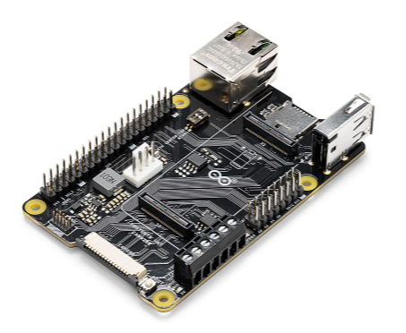
ASX00049

Arduino

* $43.36 - * $50.36

IN STOCK 2847
Buy

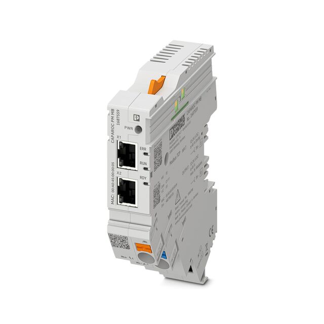
1687559

Phoenix Contact Ltd

[no prices available]

IN STOCK 2
Buy

Reference Designs

RD006

Wurth Elektronik

RD006 - 3 W Dual-output isolated auxiliary supply for communication interfaces and measurement systems

CN0583

Analog Devices Inc.

Multistandard Micropower Verified Smoke Detection System-on-Module

Technical Resources

EVALUATION KITS

EVAL-AD7124-8SDZ

Analog Devices Inc.

$0.00 - * $79.12

IN STOCK 792
Buy
View All