
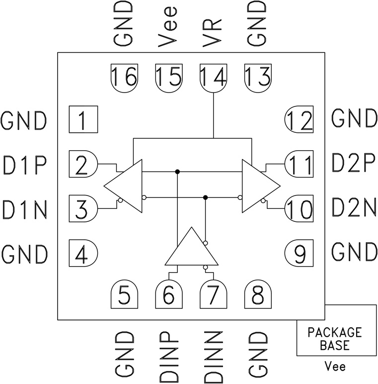
118777-HMC678LC3C
Analog Devices Inc.The HMC678LC3C is a 2:1 Selector designed to support data transmission rates of up to 13 Gbps, and selector port operation of up to 13 GHz. The selector routes one of the two single-ended inputs to the differential output upon assertion of the proper select port. All single-ended input signals to the HMC678LC3C are terminated with 50 ohms to ground on-chip, and may be either AC or DC coupled.The outputs of the HMC678LC3C may be operated either differentially or single-ended. Outputs can be connected directly to a 50 ohm terminated system, while DC blocking capacitors may be used if the terminating system is 50 ohms to a non-ground DC voltage. The HMC678LC3C operates from a single -3.3V dc supply and is available in a ceramic RoHS compliant 3x3 mm SMT package.APPLICATIONS 2:1 Multiplexer up to 13 Gbps RF ATE Applications Broadband Test & Measurement Serial Data Transmission up to 13 Gbps Redundant Path Switching Built-in Test
118777-HMC720LP3E
Analog Devices Inc.The HMC720LP3E is a 1:2 Fanout Buffer designed to support data transmission rates up to 14 Gbps, and clock frequencies as high as 14 GHz.All differential inputs to the HMC720LP3E are CML and terminated on-chip with 50 Ohms to the positive supply, GND, and may be DC or AC coupled. Outputs can be connected directly to a 50 Ohm ground-terminated system or drive devices with CML logic input. The HMC720LP3E also features an ouput level control pin, VR, which allows for loss compensation or signal level optimization. The HMC720LP3E operates from a single -3.3 V supply and is available in ROHS-compliant 3x3 mm SMT package.?APPLICATIONS 16 G Fiber Channel RF ATE Applications Broadband Test & Measurement Serial Data Transmission?up to 13 Gbps Clock Buffering up to 13 GHz

120257-HMC613LC4B
Analog Devices Inc.The HMC613LC4B is a Successive Detection Log Video Amplifier (SDLVA) which operates from 0.1 to 20 GHz. The HMC613LC4B provides a logging range of 59 dB. This device offers typical fast rise/fall times of 4/18 ns and a superior delay time of 14 ns. The HMC613LC4B log video output slope is typically 14 mV/dB. Maximum recovery times are less than 30 ns. The HMC613LC4B is available in a highly compact 4x4 mm SMT ceramic package and is ideal for high speed channelized receiver applications.APPLICATIONS EW, ELINT & IFM Receivers DF Radar Systems ECM Systems Broadband Test & Measurement Power Measurement & Control Circuits Military & Space Applications

122520-HMC724LC3
Analog Devices Inc.The HMC724 is a 1:2 Fanout Buffer designed to support data transmission rates up to 14 Gbps, and clock frequencies as high as 14 GHz. All differential inputs and outputs are DC coupled and terminated on chip with 50 Ohm resistors to ground. The outputs may be used in either single ended or differential modes, and should be AC or DC coupled into 50 Ohm resistors connected to ground.All differential inputs to the HMC724 are CML and terminated on-chip with 50 Ohms to the positive supply, GND, and may be DC or AC coupled. The differential CMl outputs are source terminated to to 50 Ohms and may also be AC or DC coupled. Outputs can be connected directly to a 50 Ohm ground-terminated system or drive devices with CML logic input. The HMC724 operates from a single -3.3 V supply and is available in ROHS-compliant 3x3 mm SMT package.APPLICATIONS 16 G Fiber Channel RF ATE Applications Broadband Test & Measurement Serial Data Transmission up to 14 Gbps Clock Buffering up to 14 GHz

122520-HMC727LC3C
Analog Devices Inc.The HMC727 is a D-type Flip Flop designed to support data transmission rates of up to 13 Gbps, and clock frequencies as high as 13 GHz. During normal operation, data is transferred to the outputs on the positive edge of the clock. Reversing the clock inputs allows for negative-edge triggered applications. All input signals to the HMC727 are terminated with 50 Ohms to ground on-chip, and maybe either AC or DC coupled.The differential outputs of the HMC727 may be either AC or DC coupled. Outputs can be connected directly to a 50 Ohm to ground terminated system, while DC blocking capacitors may be used if the terminating system is 50 Ohms to a nonground DC voltage. The HMC727 operates from a single -3.3V DC supply and is available in a ceramic RoHS compliant 3x3 mm SMT package.APPLICATIONS RF ATE Applications Broadband Test & Measurement Serial Data Transmission?up to 13 Gbps Digital Logic Systems up to 13 GHz

123987-HMC737LP4
Analog Devices Inc.The HMC737 is a GaAs InGaP Heterojunction Bipolar Transistor (HBT) MMIC VCO. The HMC737 integrate a resonator, negative resistance device, varactor diode and feature half frequency output. The VCO's phase noise performance is excellent over temperature, shock, and process due to the oscillator's monolithic structure. Power output is +9 dBm typical from a +4.2V supply voltage. The voltage controlled oscillator is packaged in a leadless QFN 4x4 mm surface mount package, and requires no external matching components.APPLICATIONS Point-to-Multi-Point Radios Test Equipment & Industrial Controls SATCOM Military End-Use

124390-HMC740ST89E
Analog Devices Inc.The HMC740 is an InGaP Heterojunction Bipolar Transistor (HBT) Gain Block MMIC SMT amplifier covering 0.05 to 3 GHz. Packaged in an industry standard SOT89, the amplifier can be used as a cascadable 50 Ohm RF or IF gain stage as well as a PA or LO driver with up to +18 dBm output power. The HMC740 offers 15 dB of gain with a +40 dBm output IP3 at 100 MHz, and can operate directly from a +5V supply. The HMC740 exhibits excellent gain and output power stability over temperature, while requiring a minimal number of external bias components.Applications Cellular/3G & WiMAX/4G Fixed Wireless & WLAN CATV, Cable Modem & DBS Microwave Radio & Test Equipment IF & RF Applications

125658-HMC686LP4
Analog Devices Inc.The HMC686LP4(E) is a high dynamic range passive MMIC mixer with integrated LO amplifier in a 4x4 SMT QFN package covering 0.7 to 1.1 GHz. Excellent input IP3 performance of +34 dBm for down conversion is provided for 3G & 4G GSM/CDMA applications at an LO drive of 0 dBm. With an input 1 dB compression of +25 dBm, the RF port will accept a wide range of input signal levels. Conversion loss is 7.5 dB typical. The DC to 500 MHz IF frequency response will satisfy GSM/CDMA transmit or receive frequency plans.The HMC686LP4(E) is optimized to high side LO frequency plans for 0.7 - 1.1 GHz RF Band and is pin for pin compatible with the?HMC684LP4(E)?which is a 0.7 - 1.0 GHz converter optimized for low side LO. The HMC686LP4(E) is optimized to low side LO frequency plans for 1.4 - 1.5 GHz RF LTE band applications.APPLICATIONS Cellular/3G & LTE/WiMAX/4G Basestations & Repeaters GSM, CDMA & OFDM Transmitters and Receivers

126578-HMC854LC5
Analog Devices Inc.The HMC854LC5 is a 4:1 multiplexer designed for 28 Gbps data serialization. The mux latches the four differential inputs on a rising edge of the input clock. The device uses both rising and falling edges of the half-rate clock to serialize the data. A quarter-rate clock output generated on chip can be used to synchronize data into the mux. The mux is DC coupled supporting broadband operation.All clock and data inputs to the HMC854LC5 are CML and terminated on-chip with 50 Ohms to the positive supply, GND, and may be DC or AC coupled. The differential outputs are source terminated to 50 Ohms and may also be AC or DC coupled. Outputs can be connected directly to a 50 Ohm ground terminated system, or drive devices with CML logic input. The HMC854LC5 also features an output level control pin, VR, which allows for loss compensation or signal level optimization. The HMC854LC5 operates from a single -3.3V supply and is available in ROHS compliant 5x5 mm SMT package.APPLICATIONS SONET OC-192 Broadband Test & Measurement Serial Data Transmission?up to 28 Gbps Mux Modes: 4:1 @ 28 Gbps NRZ 2:1 @ 14 Gbps RZ and NRZ FPGA Interfacing

128159-HMC822LP6CE
Analog Devices Inc.The HMC822LP6CE is a fully functioned Fractional-N Phase-Locked-Loop (PLL) Frequency Synthesizer with an Integrated Voltage Controlled Oscillator (VCO). The synthesizer consists of an integrated low noise VCO with a triband output, an autocalibration subsystem for low voltage VCO tuning, a very low noise digital Phase Detector (PD), a precision controlled charge pump, a low noise reference path divider and a fractional divider.The fractional synthesizer features an advanced delta-sigma modulator design that allows both ultra-fine step sizes and low spurious products. The phase detector (PD) features cycle slip prevention (CSP) technology to allow faster frequency hopping times. Ultra low in-close phase noise and low spurious also allows wider loop bandwidths for faster frequency hopping and low micro-phonics.For theory of operation and register map refer to the 'PLLs with Integrated VCO - RF VCOs' Operating Guide.Applications Cellular/4G Infrastructure Repeaters and Femtocells Communications Test Equipment CATV Equipment Phased Array Applications DDS Replacement? Very High Data Rate Radios
129467-HMC820LP6CE
Analog Devices Inc.The HMC820LP6CE is a fully functioned Fractional-N Phase-Locked-Loop (PLL) Frequency Synthesizer with an Integrated Voltage Controlled Oscillator (VCO). The synthesizer consists of an integrated low noise VCO with a triband output, an autocalibration subsystem for low voltage VCO tuning, a very low noise digital Phase Detector (PD), a precision controlled charge pump, a low noise reference path divider and a fractional divider.The fractional synthesizer features an advanced delta-sigma modulator design that allows both ultra-fine step sizes and low spurious products. The phase detector (PD) features cycle slip prevention (CSP) technology to allow faster frequency hopping times. Ultra low in-close phase noise and low spurious also allows wider loop bandwidths for faster frequency hopping and low micro-phonics.For theory of operation and register map refer to the 'PLLs with Integrated VCO - RF VCOs' Operating Guide.Applications Cellular/4G Infrastructure Repeaters and Femtocells Communications Test Equipment CATV Equipment Phased Array Applications DDS Replacement? Very High Data Rate Radios
129468-HMC820LP6CE
Analog Devices Inc.The HMC820LP6CE is a fully functioned Fractional-N Phase-Locked-Loop (PLL) Frequency Synthesizer with an Integrated Voltage Controlled Oscillator (VCO). The synthesizer consists of an integrated low noise VCO with a triband output, an autocalibration subsystem for low voltage VCO tuning, a very low noise digital Phase Detector (PD), a precision controlled charge pump, a low noise reference path divider and a fractional divider.The fractional synthesizer features an advanced delta-sigma modulator design that allows both ultra-fine step sizes and low spurious products. The phase detector (PD) features cycle slip prevention (CSP) technology to allow faster frequency hopping times. Ultra low in-close phase noise and low spurious also allows wider loop bandwidths for faster frequency hopping and low micro-phonics.For theory of operation and register map refer to the 'PLLs with Integrated VCO - RF VCOs' Operating Guide.Applications Cellular/4G Infrastructure Repeaters and Femtocells Communications Test Equipment CATV Equipment Phased Array Applications DDS Replacement? Very High Data Rate Radios
129472-HMC822LP6CE
Analog Devices Inc.The HMC822LP6CE is a fully functioned Fractional-N Phase-Locked-Loop (PLL) Frequency Synthesizer with an Integrated Voltage Controlled Oscillator (VCO). The synthesizer consists of an integrated low noise VCO with a triband output, an autocalibration subsystem for low voltage VCO tuning, a very low noise digital Phase Detector (PD), a precision controlled charge pump, a low noise reference path divider and a fractional divider.The fractional synthesizer features an advanced delta-sigma modulator design that allows both ultra-fine step sizes and low spurious products. The phase detector (PD) features cycle slip prevention (CSP) technology to allow faster frequency hopping times. Ultra low in-close phase noise and low spurious also allows wider loop bandwidths for faster frequency hopping and low micro-phonics.For theory of operation and register map refer to the 'PLLs with Integrated VCO - RF VCOs' Operating Guide.Applications Cellular/4G Infrastructure Repeaters and Femtocells Communications Test Equipment CATV Equipment Phased Array Applications DDS Replacement? Very High Data Rate Radios

129475-HMC828LP6CE
Analog Devices Inc.The HMC828LP6CE is a fully functioned Fractional-N Phase-Locked-Loop (PLL) Frequency Synthesizer with an Integrated Voltage Controlled Oscillator (VCO). The synthesizer consists of an integrated low noise VCO with divide-by-2 output, an autocalibration subsystem for low voltage VCO tuning, a very low noise digital Phase Detector (PD), a precision controlled charge pump, a low noise reference path divider and a fractional divider.The fractional synthesizer features an advanced delta-sigma modulator design that allows both ultra-fine step sizes and low spurious products. The phase detector (PD) features cycle slip prevention (CSP) technology to allow faster frequency hopping times. Ultra low in-close phase noise and low spurious also allows wider loop bandwidths for faster frequency hopping and low micro-phonics.For theory of operation and register map refer to the 'PLLs w/ Integrated VCO - RF VCOs' Operating Guide.Applications Cellular/4G Infrastructure Repeaters and Femtocells Communications Test Equipment CATV Equipment Phased Array Applications DDS Replacement? Very High Data Rate Radios

129512-HMC838LP6CE
Analog Devices Inc.The HMC838LP6CE is a fully functioned Fractional-N Phase-Locked-Loop (PLL) Frequency Synthesizer with an Integrated Voltage Controlled Oscillator (VCO). The synthesizer consists of an integrated low noise VCO with a triband output, an autocalibration subsystem for low voltage VCO tuning, a very low noise digital Phase Detector (PD), a precision controlled charge pump, a low noise reference path divider and a fractional divider.The fractional synthesizer features an advanced delta-sigma modulator design that allows both ultra-fine step sizes and low spurious products. The phase detector (PD) features cycle slip prevention (CSP) technology to allow faster frequency hopping times. Ultra low in-close phase noise and low spurious also allows wider loop bandwidths for faster frequency hopping and low micro-phonics.For theory of operation and register map refer to the 'PLLs with Integrated VCO - RF VCOs' Operating Guide.Applications Cellular/4G Infrastructure Repeaters and Femtocells Communications Test Equipment CATV Equipment Phased Array Applications DDS Replacement? Very High Data Rate Radios

129514-HMC839LP6CE
Analog Devices Inc.The HMC839LP6CE is a fully functioned Fractional-N Phase-Locked-Loop (PLL) Frequency Synthesizer with an Integrated Voltage Controlled Oscillator (VCO). The synthesizer consists of an integrated low noise VCO with a triband output, an autocalibration subsystem for low voltage VCO tuning, a very low noise digital Phase Detector (PD), a precision controlled charge pump, a low noise reference path divider and a fractional divider.The fractional synthesizer features an advanced delta-sigma modulator design that allows both ultra-fine step sizes and low spurious products. The phase detector (PD) features cycle slip prevention (CSP) technology to allow faster frequency hopping times. Ultra low in-close phase noise and low spurious also allows wider loop bandwidths for faster frequency hopping and low micro-phonics.For theory of operation and register map refer to the 'PLLs with Integrated VCO - RF VCOs' Operating Guide.Applications Cellular/4G Infrastructure Repeaters and Femtocells Communications Test Equipment CATV Equipment Phased Array Applications DDS Replacement? Very High Data Rate Radios

129538-HMC974LC3C
Analog Devices Inc.The HMC974LC3C is a silicon germanium (SiGe) monolithic, ultra fast window comparator that features reduced swing positive emitter-coupled logic (RSPECL) output drivers that are level latched. Three output ports detect whether an analog input signal is above, below, or between two reference levels supplied at the input.The outputs are single-ended negative logic. Incorporating two proven comparators at the input provides good dc and dynamic matching and reduces the input capacitance. The reduced swingoutput stages are designed to directly drive 400 mV into 50 ? terminated to a voltage (VTERM = VCCO ? 2 V).HMC974LC3C features high speed latches that can either be enabled to latch the output data or left in the track mode toimplement a tracking window comparator.Applications Automatic test equipment (ATE) High speed instrumentation Clock and data restoration Semiconductor test systems Threshold detection in electronic warfare systems

130369-HMC767LP6CE
Analog Devices Inc.The HMC767LP6CE is a fully functioned Fractional-N Phase-Locked-Loop (PLL) Frequency Synthesizer with an integrated Voltage Controlled Oscillator (VCO). The input reference frequency range is DC to 350 MHz while the advanced delta-sigma modulator design in the fractional synthesizer allows both ultra-fine step sizes and very low spurious products. The highly integrated structure provides excellent phase noise performance over temperature, shock and process. In addition, the HMC767LP6CE offers frequency sweep and modulation features, external triggering, double-buffering, exact frequency control, phase modulation and more. The HMC767LP6CE is packaged in a leadless QFN 6 x 6 mm surface mount package.For theory of operation and register map refer to the 'PLLs w/ Integrated VCO - Microwave VCOs' Operating Guide.Applications VSAT Radio Microwave Point-To-Point Radios Test Equipment & Industrial Control Military End-Use Phased Array Applications FMCW Radar Systems

130437-HMC1010LP4E
Analog Devices Inc.The HMC1010LP4E Power Detector is designed for RF power measurement, and control applications for frequencies up to 3.9 GHz. The detector provides an accurate RMS representation of any RF/IF input signal. The output is a temperature compensated monotonic, representation of real signal power, measured with an input sensing range of 60 dB.The HMC1010LP4E is ideally suited to those wide bandwidth, wide dynamic range applications, requiring repeatable measurement of real signal power, especially where RF/IF wave shape and/or crest factor change with time.The integration bandwidth of the HMC1010LP4E is digitally programmable with the use of input pins SC I1- 4 with a range of more than 4 decades. This allows the user to dynamically set the operation bandwidth providing the capability of handling different types of modulations on the same platform.The HMC1010LP4E features an internal op-amp at output stage, which provides for slope & intercept adjustments and enables controller application.Applications Log ?> Root-Mean-Square?(RMS) Conversion Received Signal Strength?Indication (RSSI) Transmitter Signal Strength?Indication (TSSI) RF Power Amplifier Efficiency Control Receiver Automatic Gain Control Transmitter Power Control

130602-HMC942LP4E
Analog Devices Inc.The HMC942LP4E is a x2 active broadband frequency multiplier utilizing GaAs pHEMT technology in a leadless RoHS compliant SMT package. When driven by a +4 dBm signal, the multiplier provides +17 dBm typical output power from 13 to 24.6 GHz. The Fo and 3Fo isolations are >20 dBc at 19 GHz. The HMC942LP4E is ideal for use in LO multiplier chains for Pt-to-Pt & VSAT Radios yielding reduced parts count vs. traditional approaches.APPLICATIONS Clock Generation Applications: SONET OC-192 & SDH STM-64 Point-to-Point & VSAT Radios Test Instrumentation Military & Space Sensors


