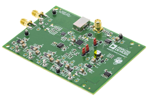
DC2141A
Analog Devices Inc.The LTM4647 is a complete 30A output switching mode step-down DC/DC ?Module? (power module) regulator. Included in the package are the switching controller, power FETs, inductor and all supporting components. Operating over an input voltage range of 4.7V to 15V, the LTM4647 supports an output voltage range of 0.6V to 1.8V, set by a single external resistor. Only a few input and output capacitors are needed.Its high efficiency design delivers 87% efficiency from 12V input to 1.0V output with 30A continuous load current. High switching frequency and a current-mode architecture enable a very fast transient response to line and load changes without sacrificing stability. The device supports frequency synchronization, programmable multiphase operation, N+1 phase redundancy, and output voltage tracking for supply rail sequencing.Fault protection features include overvoltage and overcurrent protection. The power module is offered in a space saving 9mm ? 15mm ? 5.01mm BGA package. The LTM4647 is available with SnPb (BGA) or RoHS compliant terminal finish.Applications Telecom, Networking and Industrial Equipment Point of Load Regulation
DC2147A
Analog Devices Inc.The LTM4631 is a dual 10A or single 20A output switching mode step-down DC/DC ?Module? (power module) regulator. Included in the package are the switching controller, power FETs, inductors and all supporting components. Operating from an input voltage range of 4.5V to 15V, the LTM4631 supports two outputs each with an output voltage range of 0.6V to 1.8V, each set by a single external resistor. Its high efficiency design delivers up to 10A continuous current for each output. Only a few input and output capacitors are needed.The device supports frequency synchronization, multiphase operation, Burst Mode operation and output voltage tracking for supply rail sequencing and has an onboard temperature diode for device temperature monitoring. High switching frequency and a current mode architecture enable a very fast transient response to line and load changes without sacrificing stability.Fault protection features include overvoltage and overcurrent protection. The LTM4631 is offered in an ultrathin 16mm ? 16mm ? 1.91mm LGA and 16mm x 16mm x 2.51mm BGA packages. The LTM4631 is available with SnPb (BGA) or ROHS compliant terminal finish.Applications Telecom and Networking Equipment Storage and ATCA Cards Industrial Equipment
DC2152A
Analog Devices Inc.The LTM4630A is a dual 18A or single 36A output switchingmode step-down DC/DC ?Module? (micromodule)regulator with wider VOUT range and higher efficiencythan LTM4630. Included in the package are the switchingcontrollers, power FETs, inductors and all supportingcomponents. Operating from an input voltage range of4.5V to 18V, the LTM4630A supports two outputs eachwith an output voltage range of 0.6V to 8V, each set by asingle external resistor. Its high efficiency design deliversup to 18A continuous current for each output. Only a fewinput and output capacitors are needed. The LTM4630Ais pin compatible with the LTM4620 and LTM4620A (dual13A, single 26A) and the LTM4630 (dual 18A, single 36A).The device supports frequency synchronization, multiphaseoperation, Burst Mode operation and output voltagetracking for supply rail sequencing and has an onboardtemperature diode for device temperature monitoring. Highswitching frequency and a current mode architecture enablea very fast transient response to line and load changeswithout sacrificing stability.Fault protection features include overvoltage andovercurrent protection. The LTM4630A is offered in 16mm? 16mm ? 4.41mm LGA and 16mm ? 16mm ? 5.01mmBGA packages.*Maximum VIN = 15V and VOUT = 5.3V with date code before 1720 Features VOUT LTM4630 0.6V to 1.8V LTM4630-1 0.8% DC and 3% Transient Accuracy 0.6V to 1.8V LTM4630A Higher Light Load Efficiency 0.6V to 5.3V Applications Telecom and Networking Equipment Storage and ATCA Cards Industrial Equipment
DC2153A
Analog Devices Inc.The LTC6430-15 is a differential gain block amplifier designed to drive high resolution, high speed ADCs with excellent linearity beyond 1000MHz and with low associated output noise. The LTC6430-15 operates from a single 5V power supply and consumes only 800mW.In its differential configuration, the LTC6430-15 can directly drive the differential inputs of an ADC. Using 1:2 baluns, the device makes an excellent 50? wideband balanced amplifier. While using 1:1.33 baluns, the device makes a high fidelity 50MHz to 1000MHz 75? CATV amplifier.The LTC6430-15 is designed for ease of use, requiring a minimum of support components. The device is internally matched to 100? differential source/load impedance. On-chip bias and temperature compensation ensure consistent performance over environmental changes.The LTC6430-15 uses a high performance SiGe BiCMOS process for excellent repeatability compared with similar GaAs amplifiers. All A-grade LTC6430-15 devices are tested and guaranteed for OIP3 at 240MHz. The LTC6430-15 is housed in a 4mm ? 4mm, 24-lead, QFN package with an exposed pad for thermal management and low inductance. For a single-ended 50? IF gain block with similar performance, see the related LTC6431-15.Applications Differential ADC Driver Differential IF Amplifier OFDM Signal Chain Amplifier 50? Balanced IF Amplifier 75? CATV Amplifier 700MHz to 800MHz LTE Amplifier
DC2171A-A
Analog Devices Inc.The LTM4623 is a complete 3A step-down switchingmode ?Module (micromodule) regulator in a tiny ultrathin6.25mm ? 6.25mm ? 1.82mm LGA and 6.25mm ? 6.25mm? 2.42mm BGA packages. Included in the package are theswitching controller, power FETs, inductor and supportcomponents. Operating over an input voltage range of4V to 20V or 2.375V to 20V with an external bias supply,the LTM4623 supports an output voltage range of 0.6V to5.5V, set by a single external resistor. Its high efficiencydesign delivers 3A continuous output current. Only ceramicinput and output capacitors are needed.The LTM4623 supports selectable discontinuous modeoperation and output voltage tracking for supply rail sequencing.Its high switching frequency and current modecontrol enable a very fast transient response to line andload changes without sacrificing stability. Fault protection features include overvoltage, overcurrentand overtemperature protection.The LTM4623 is available with SnPb (BGA) or RoHScompliant terminal finish.APPLICATIONS PCIe and Backside PCB Mounting Telecom, Datacom, Networking and Industrial Equipment Data Storage Rack Units and Cards
DC2171A-B
Analog Devices Inc.The LTM4625 is a complete 5A step-down switching mode ?Module (Power Module) regulator in a tiny 6.25mm ? 6.25mm ? 5.01mm BGA package. Included in the package are the switching controller, power FETs, inductor and support components. Operating over an input voltage range of 4V to 20V or 2.375V to 20V with an external bias supply, the LTM4625 supports an output voltage range of 0.6V to 5.5V, set by a single external resistor. Its high efficiency design delivers up to 5A continuous output current. Only bulk input and output capacitors are needed.The LTM4625 supports selectable discontinuous mode operation and output voltage tracking for supply rail sequencing. Its high switching frequency and current mode control enable a very fast transient response to line and load changes without sacrificing stability.Fault protection features include overvoltage, overcurrent and overtemperature protection.The LTM4625 is available with SnPb or RoHS compliant terminal finish.APPLICATIONS Telecom, Datacom, Networking and Industrial?Equipment Medical Diagnostic Equipment Data Storage Rack Units and Cards Test and Debug Systems
LTC3882EUJ Demo Board | 7V ≤ VIN ≤ 14V; 0.5V ≤ VOUT0 ≤ 2V @ 35A, 0.5V ≤ VOUT1 ≤ 2V @ 35A
Analog Devices Inc.Demonstration circuit 2174A-A is a high current, high efficiency, dual-phase dual-output synchronous buck converter featuring the LTC3882EUJ, a dual output voltage mode controller. The DC2174A-A operates with a 7V to 14V input voltage and is configured for 1.5V at 35A and 1V at 35A. The output voltage adjustment range is 0.5V to 2V. The LTC3882 has the PMBus interface and power system management functions.
LTC3882EUJ Demo Board | Dual Phase Single Output PMBus Buck, 7V ≤ VIN ≤ 14V; 0.5V ≤ VOUT0 ≤ 2V @ 70A
Analog Devices Inc.Demonstration circuit 2174A-B is a high current, high efficiency, dual-phase single-output synchronous buck converter featuring the LTC3882EUJ, a dual output voltage mode controller. The DC2174A-B operates with a 7V to 14V input voltage and is configured for 1V output at 70A. The output voltage adjustment range is 0.5V to 2V. The LTC3882 has the PMBus interface and power system management functions.
DC2193A
Analog Devices Inc.The LT6118 is a complete high side current sense device that incorporates a precision current sense amplifier, an integrated voltage reference and a latching comparator. The comparator latch functionality can be enabled or disabled and the comparator can be configured to reset upon power-on. The input and the open-drain output of the comparator are independent from the current sense amplifier. The comparator trip point and amplifier gain are configured with external resistors.The overall propagation delay of the LT6118 is typically only 1.4?s, allowing for quick reaction to overcurrent conditions. The 1MHz bandwidth allows the LT6118 to be used for error detection in critical applications such as motor control. The high threshold accuracy of the comparator, combined with the ability to latch the comparator, ensures the LT6118 can capture high speed events.The LT6118 is fully specified for operation from ?40?C to 125?C, making it suitable for industrial and automotive applications. The LT6118 is available in the small 8-lead MSOP and 8-lead DFN packages.Applications Overcurrent and Fault Detection Current Shunt Measurement Battery Monitoring Motor Control Automotive Monitoring and Control Industrial Control
DC2199A-A
Analog Devices Inc.The LTC3766 is a PolyPhase-capable secondary-side controller for synchronous forward converters. When used in conjunction with the LTC3765 active-clamp forward controller and gate driver, the part creates a complete isolated power supply that combines the power of multiphase operation with the speed of secondary-side control.The LTC3766 has been designed to simplify the design of active clamp forward converters. Working in concert with the LTC3765, the LTC3766 forms a robust, self-starting converter that eliminates the need for the separate bias regulator that is commonly used in secondary-side control applications. A precision current-limit coupled with clean start-up into a pre-biased load make the LTC3766 an excellent choice for high-power battery charger applications.The LTC3766 provides extensive remote sensing and output protection features, while Direct Flux Limit guarantees no transformer saturation without compromising transient response. A linear regulator controller and internal bypass LDO are also provided to simplify the generation of the secondary-side bias voltage.Applications Isolated 48V Telecommunication Systems Isolated Battery Chargers Automotive and Military Systems Industrial, Avionics and Heavy Equipment
DC2199A-B
Analog Devices Inc.The LTC3766 is a PolyPhase-capable secondary-side controller for synchronous forward converters. When used in conjunction with the LTC3765 active-clamp forward controller and gate driver, the part creates a complete isolated power supply that combines the power of multiphase operation with the speed of secondary-side control.The LTC3766 has been designed to simplify the design of active clamp forward converters. Working in concert with the LTC3765, the LTC3766 forms a robust, self-starting converter that eliminates the need for the separate bias regulator that is commonly used in secondary-side control applications. A precision current-limit coupled with clean start-up into a pre-biased load make the LTC3766 an excellent choice for high-power battery charger applications.The LTC3766 provides extensive remote sensing and output protection features, while Direct Flux Limit guarantees no transformer saturation without compromising transient response. A linear regulator controller and internal bypass LDO are also provided to simplify the generation of the secondary-side bias voltage.Applications Isolated 48V Telecommunication Systems Isolated Battery Chargers Automotive and Military Systems Industrial, Avionics and Heavy Equipment
DC2199B-C
Analog Devices Inc.The LTC3766 is a PolyPhase-capable secondary-side controller for synchronous forward converters. When used in conjunction with the LTC3765 active-clamp forward controller and gate driver, the part creates a complete isolated power supply that combines the power of multiphase operation with the speed of secondary-side control.The LTC3766 has been designed to simplify the design of active clamp forward converters. Working in concert with the LTC3765, the LTC3766 forms a robust, self-starting converter that eliminates the need for the separate bias regulator that is commonly used in secondary-side control applications. A precision current-limit coupled with clean start-up into a pre-biased load make the LTC3766 an excellent choice for high-power battery charger applications.The LTC3766 provides extensive remote sensing and output protection features, while Direct Flux Limit guarantees no transformer saturation without compromising transient response. A linear regulator controller and internal bypass LDO are also provided to simplify the generation of the secondary-side bias voltage.Applications Isolated 48V Telecommunication Systems Isolated Battery Chargers Automotive and Military Systems Industrial, Avionics and Heavy Equipment
DC2211A
Analog Devices Inc.The LTC2983 measures a wide variety of temperature sensors and digitally outputs the result, in ?C or ?F, with 0.1?C accuracy and 0.001?C resolution. The LTC2983 can measure the temperature of virtually all standard (type B, E, J, K, N, S, R, T) or custom thermocouples, automatically compensate for cold junction temperatures and linearize the results. The device can also measure temperature with standard 2-, 3- or 4-wire RTDs, thermistors and diodes. It has 20 reconfigurable analog inputs enabling many sensor connections and configuration options. The LTC2983 includes excitation current sources and fault detection circuitry appropriate for each type of temperature sensor.The LTC2983 allows direct interfacing to ground referenced sensors without the need for level shifters, negative supply voltages, or external amplifiers. All signals are buffered and simultaneously digitized with three high accuracy, 24-bit ?? ADCs, driven by an internal 10ppm/?C (maximum) reference.Applications Direct Thermocouple Measurements Direct RTD Measurements Direct Thermistor Measurements Custom Sensor Applications
DC2212A
Analog Devices Inc.The LTC2983 measures a wide variety of temperature sensors and digitally outputs the result, in ?C or ?F, with 0.1?C accuracy and 0.001?C resolution. The LTC2983 can measure the temperature of virtually all standard (type B, E, J, K, N, S, R, T) or custom thermocouples, automatically compensate for cold junction temperatures and linearize the results. The device can also measure temperature with standard 2-, 3- or 4-wire RTDs, thermistors and diodes. It has 20 reconfigurable analog inputs enabling many sensor connections and configuration options. The LTC2983 includes excitation current sources and fault detection circuitry appropriate for each type of temperature sensor.The LTC2983 allows direct interfacing to ground referenced sensors without the need for level shifters, negative supply voltages, or external amplifiers. All signals are buffered and simultaneously digitized with three high accuracy, 24-bit ?? ADCs, driven by an internal 10ppm/?C (maximum) reference.Applications Direct Thermocouple Measurements Direct RTD Measurements Direct Thermistor Measurements Custom Sensor Applications
LTC3877 Demo Board | Dual Buck Controller, Sub-mΩ DCR Sensing, 6V ≤ VIN ≤ 14V, VOUT1 is VID Programmable from 0.6V to 1.23V @ 30A, VOUT2 is 1.5V @ 30A
Analog Devices Inc.Demonstration circuits 2229A-A and 2229A-B feature the LTC3877 in two high output current, high efficiency, VID programmed step-down converters with sub-mΩ DCR sensing. For both converters, the input voltage range is 6V to 14V and the switching frequency is 400kHz.
DC2240A
Analog Devices Inc.The LT8714 is a synchronous PWM DC/DC controller designed for a four quadrant output converter. The output voltage cleanly transitions through zero volts with sourcing and sinking output current capability.The LT8714 is ideal for regulating to positive, negative, or zero volts when configured for the novel four quadrant topology. Applications include four quadrant power supplies, high power bidirectional current sources, active loads, and high power, low frequency signal amplification. In addition, the LT8714 incorporates a power good feature to let the user know if VOUT is above or below its target regulation voltage.The LT8714?s switching frequency range can be programmed between 100kHz and 750kHz via a resistor from the RT pin to GND. A SYNC pin is also provided if the user would like to synchronize the part to an external clock. Additional features such as current limiting and soft-start are included. The LT8714 is available in a 20?lead TSSOP package.Applications Four Quadrant Power Supplies Bidirectional Current Sources High Power, Low Frequency Signal Amplification Test and Measurement Electronic Window Tinting
DC2253A
Analog Devices Inc.The LTC3789 is a high performance buck-boost switching regulator controller that operates from input voltages above, below or equal to the output voltage. The constant-frequency, current mode architecture allows a phase-lockable frequency of up to 600kHz, while an output current feedback loop provides support for battery charging. With a wide 4V to 38V (40V maximum) input and output range and seamless, low noise transitions between operating regions, the LTC3789 is ideal for automotive, telecom and battery-powered systems.The operating mode of the controller is determined through the MODE/PLLIN pin. The MODE/PLLIN pin can select between pulse-skipping mode and forced continuous mode operation and allows the IC to be synchronized to an external clock. Pulse-skipping mode offers high efficiency and low ripple at light loads, while forced continuous mode operates at a constant frequency for noise-sensitive applications.A PGOOD pin indicates when the output is within 10% of its designed set point. The LTC3789 is available in low profile 28-pin 4mm ? 5mm QFN and narrow SSOP packages.Applications Automotive Systems Distributed DC Power Systems High Power Battery-Operated Devices Industrial Control
DC2255A
Analog Devices Inc.The LTC3106 is a highly integrated, ultralow voltage buck-boost DC/DC converter with automatic PowerPath management optimized for multisource, low power systems. At no load, the LTC3106 draws only 1.6?A while creating an output voltage up to 5V from either input source.If the primary power source is unavailable, the LTC3106 seamlessly switches to the backup power source. The LTC3106 is compatible with either rechargeable or primary cell batteries and can trickle charge a backup battery whenever there is an energy surplus available. Optional maximum power point control ensures power transfer is optimized between power source and load. The output voltage and backup voltage, VSTORE, are programmed digitally, reducing the required number of external components. Zero power Shelf Mode ensures that the backup battery will remain charged if left connected to the LTC3106 for an extended time.Additional features include an accurate turn-on voltage, a power good indicator for VOUT, a user selectable 100mA peak current limit setting for lower power applications, thermal shutdown as well as user selectable backup power and output voltages.Applications Wireless Sensor Networks Home or Office Building Automation Energy Harvesting Remote Sensors
EV1HMC3716LP4
Analog Devices Inc.The HMC3716LP4E is a digital phase frequency detector which operates from 10 to 1300MHz. It is intended for usein low phase noise synthesizer applications.The combination of high frequency of operation along with its ultra low phase noise floor make possible synthesizerswith wide loop bandwidth and low N resulting in fast switching and very low phase noise. When used in conjunctionwith a differential loop amplifier, the HMC3716LP4E generates output voltages that can be used to phase lock a VCOto a reference oscillator.The device is packaged in a 24-pin, 4 x 4mm leadless QFN surface mount package with an exposed ground paddlefor improved RF and thermal performance.Applications Point-to-point radios Satellite communication systems Military applications Sonet clock generation
EV1HMC539ALP3
Analog Devices Inc.The HMC539ALP3/539ALP3E is a broadband5-bit GaAs IC digital attenuator in a low cost leadless surface mount package. This single positive control line per bit digital attenuator utilizes an offchip AC ground capacitor for near DC operation,making it suitable for a wide variety of RF and IFapplications. Covering DC to 4 GHz, the insertion loss is less than 0.7 dB typical. The attenuatorbit values are 0.25 (LSB), 0.5, 1, 2, and 4 dB for atotal attenuation of 7.75 dB. Attenuation accuracy isexcellent at ? 0.05 dB typical step error. The attenu-ator also features a high IIP3 of +62 dBm. Five TTL/CMOS control inputs are used to select each attenuation state. A single Vdd bias of +3V to +5V is required.Applications Cellular infrastructure ISM, MMDS, WLAN, WiMAX, WiBro Microwave radio and VSAT Test equipment and sensors


