Top Manufacturers
Stock

Displaying 541 - 560 of 5453

Evaluation Kits from Analog Devices Inc.

EVAL-ADM1170EBZ

Analog Devices Inc.
The ADM1170 is a Hot Swap controller that allows a board to be safely inserted and removed from a live backplane. This is achieved using a pass FET with a current control loop that monitors the input current using a sense resistor. An internal charge pump is used to enhance the gate of theexternal high side N-channel FET. When an over current condition is detected the gate voltage of the FET is reduced to limit the current flowing through the sense resistor. The ADM1170 operates with a supply voltage ranging from 2.7V to 16.5V. Using separate SENSE pins from VCC the ADM1170 allows for the hot swap of supplies ranging down to 1.6V. During an overcurrent condition the timer cap determines the amount of time the FET will remain in this condition. The ON (ON-CLR) pin is the enable input for the device and also acts as a latched fault reset for the ADM1170-2 model. The SS pin is used to control the inrush current profile by ramping up the current sense limit at a rate set by the SS capacitor. This device is available in two options: the ADM1170-1 will automatic retry for over-current fault and the ADM1170-2 will latch-off for an over-current fault. The ADM1170 is packaged in an 8-lead TSOT packageAPPLICATIONS Hot Swap Board Insertion ? Line Cards, Raid Systems Electronic Circuit Breaker Industrial High Side Switch/Circuit Breaker

EVAL-ADM1171EBZ

Analog Devices Inc.
The ADM1171 is a Hot Swap controller that allows a board to be safely inserted and removed from a live backplane. This is achieved using a pass FET with a current control loop that monitors the input current using a sense resistor. An internal charge pump is used to enhance the gate of theexternal high side N-channel FET. When an over current condition is detected the gate voltage of the FET is reduced to limit the current flowing through the sense resistor. The ADM1171 operates with a supply voltage ranging from 2.7V to 16.5V. During an overcurrent condition the timer capdetermines the amount of time the FET will remain in this condition. The ON (ON/CLR) pin is the enable input for the device and also acts as a latched fault reset for the ADM1171-2 model. The magnitude of the current flowing through the Sense resistor can be determined by the voltage on the CSOUT pin The SS pin allows the user to control the soft start profile of the current ramp at start-up via an external capacitor. This device is available in two options: the ADM1171-1 will automatic retry for over-current fault and the ADM1171-2 will latch-off for an over-current fault. The ADM1171 is packaged in an 8-lead TSOT package.APPLICATIONS Hot Swap Board Insertion ? Line Cards, Raid systems Electronic Circuit Breaker Industrial High Side Switch/Circuit Breaker

EVAL-ADM1178EBZ

Analog Devices Inc.
The ADM1178 is an integrated hot swap controller and current sense amplifier that offers digital current and voltage monitoring via an on-chip 12-bit analog-to-digital converter (ADC), communicated through an I2C? interface.An internal current sense amplifier measures voltage across the sense resistor in the power path via the VCC pin and the SENSE pin.The ADM1178 limits the current through this resistor by control-ling the gate voltage (via the GATE pin) of an external N-channel FET in the power path. The voltage across the sense resistor (and therefore the inrush current) is kept below a preset maximum.The ADM1178 protects the external FET by limiting the time that the maximum current runs through it. This current limit period is set by the value of the capacitor attached to the TIMER pin. Additionally, the device provides protection from overcurrent events that may occur after the hot swap event is complete. In case of a short-circuit event, the current in the sense resistor exceeds an overcurrent trip threshold, and the FET is switched off immediately by pulling down the GATE pin.A 12-bit ADC can measure the current seen in the sense resistor, as well as the supply voltage on the VCC pin. An alert output can be set to trigger when the ADC current reading exceeds a programmed overcurrent limit threshold.An industry-standard I2C interface allows a controller to read current and voltage data from the ADC. Measurements can be initiated by an I2C command. Alternatively, the ADC can run continuously, and the user can read the latest conversion data whenever it is required. Up to four unique I2C addresses can be created, depending on how the ADR pin is connected.The ADM1178 is packaged in a 10-lead MSOP.ApplicationsPower monitoring/power budgeting Central office equipment Telecommunication and data communication equipment PCs/servers

EVAL-ADM1184EBZ

Analog Devices Inc.
The ADM1184 is an integrated, 4-channel voltage-monitoring device. A 2.7 V to 5.5 V power supply is required on the VCC pin to power the device.Four precision comparators monitor four voltage rails. Each comparator has a 0.6 V reference with a worst-case accuracy of 0.8%. Resistor networks that are external to the VIN1, VIN2, VIN3, and VIN4 pins set the trip points for the monitored supply rails.The ADM1184 has four open-drain outputs. Of these outputs, OUT1 to OUT3 can be used to enable power supplies, and PWRGD is a common power-good output indicating that all monitored supplies are above their respective thresholds.OUT1 to OUT3 are dependent on their associated VINx input (that is, VIN1, VIN2, or VIN3). If a supply monitored by VINx drops below its programmed threshold, the associated OUTx pin and PWRGD are disabled.PWRGD is a common power-good output indicating the status of all monitored supplies. There is an internal 190 ms (typical) delay associated with the assertion of the PWRGD output. If VIN1, VIN2, VIN3, or VIN4 drops below its programmed threshold, PWRGD is deasserted immediately.The ADM1184 is available in a 10-lead mini small outline package (MSOP).APPLICATIONS Monitor and alarm functions Telecommunications Microprocessor systems PC/servers

EVAL-ADM1186-1MBZ

Analog Devices Inc.
The ADM1186-1 and ADM1186-2 are integrated, four-channel, voltage monitoring and sequencing devices. A 2.7 V to 5.5 V power supply is required on the VCC pin for power.Four precision comparators monitor four voltage rails, with all comparators sharing a 0.6 V reference and a worst-case accuracy of 0.8%. Resistor networks that are external to the VIN1, VIN2, VIN3, and VIN4 pins set the Under Voltage (UV) trip points for the monitored supply rails.The ADM1186-1 and ADM1186-2 have four open drain enable outputs, OUTx, that are used to enable power supplies. An open drain power good output, PWRGD, is provided that indicatesthe four VINx inputs are above their UV thresholds.A state machine monitors the state of the UP and?DOWN pins on the ADM1186-1 or the UP/overbar: DOWN pin on the ADM1186-2 to control the supply sequencing direction. In the ?Wait Start?state, a rising edge transition on the UP or UP/DOWN pin triggers a power-up sequence. A falling edge transition on the DOWN or UP/DOWN pin in the ?Power Up Done? statetriggers a power down sequence.During a power up sequence, the state machine enables each power supply in turn. The supply output voltage is monitored to determine if it rises above the UV threshold level within a userdefined duration called the blanking time. If a supply rises above the UV threshold then the next enable output in the sequence is turned on. In addition to the blanking time a user may also define sequencing time delays between each enable output turning on. When all four enable outputs are on, and the four VINx pins are above their UV trip points the power up sequence is complete. The ADM1186-1 provides an open drain pin, SEQ_DONE, that is asserted high to provide an indication that an up sequence is complete. The SEQ_DONE pins is allows multiple cascadedADM1186-1 devices to be perform controlled power up and down sequences. During a power down sequence the enable outputs turn off inreverse order. The sequence time delays between successive supplies the same as during the power up sequence, and no blanking time is used during a power down sequence. At the end of a down sequence the SEQ_DONE pin is brought low. During sequencing and when powered up, the state machine continuously monitors for any fault conditions. Faults include a UV condition on any of the inputs, or an unexpected controlinput. Any fault that occurs causes the state machine to enter a fault handler. This immediately turns off all enable outputs, and ensures that the device is ready to start a new up sequence. The ADM1186-1 has a bi-directional open drain pin, FAULT, that facilitates fault handling when using multiple devices. An ADM1186-1 experiencing a fault condition drives the FAULT pin low, causing other connected ADM1186-1devices to enter their own fault handling state.The ADM1186-1 is available in a 20-lead QSOP package andthe ADM1186-2 is available in a 16-lead QSOP package.

EVAL-ADM1186-2MBZ

Analog Devices Inc.
The ADM1186-1 and ADM1186-2 are integrated, four-channel, voltage monitoring and sequencing devices. A 2.7 V to 5.5 V power supply is required on the VCC pin for power.Four precision comparators monitor four voltage rails, with all comparators sharing a 0.6 V reference and a worst-case accuracy of 0.8%. Resistor networks that are external to the VIN1, VIN2, VIN3, and VIN4 pins set the Under Voltage (UV) trip points for the monitored supply rails.The ADM1186-1 and ADM1186-2 have four open drain enable outputs, OUTx, that are used to enable power supplies. An open drain power good output, PWRGD, is provided that indicatesthe four VINx inputs are above their UV thresholds.A state machine monitors the state of the UP and?DOWN pins on the ADM1186-1 or the UP/overbar: DOWN pin on the ADM1186-2 to control the supply sequencing direction. In the ?Wait Start?state, a rising edge transition on the UP or UP/DOWN pin triggers a power-up sequence. A falling edge transition on the DOWN or UP/DOWN pin in the ?Power Up Done? statetriggers a power down sequence.During a power up sequence, the state machine enables each power supply in turn. The supply output voltage is monitored to determine if it rises above the UV threshold level within a userdefined duration called the blanking time. If a supply rises above the UV threshold then the next enable output in the sequence is turned on. In addition to the blanking time a user may also define sequencing time delays between each enable output turning on. When all four enable outputs are on, and the four VINx pins are above their UV trip points the power up sequence is complete. The ADM1186-1 provides an open drain pin, SEQ_DONE, that is asserted high to provide an indication that an up sequence is complete. The SEQ_DONE pins is allows multiple cascadedADM1186-1 devices to be perform controlled power up and down sequences. During a power down sequence the enable outputs turn off inreverse order. The sequence time delays between successive supplies the same as during the power up sequence, and no blanking time is used during a power down sequence. At the end of a down sequence the SEQ_DONE pin is brought low. During sequencing and when powered up, the state machine continuously monitors for any fault conditions. Faults include a UV condition on any of the inputs, or an unexpected controlinput. Any fault that occurs causes the state machine to enter a fault handler. This immediately turns off all enable outputs, and ensures that the device is ready to start a new up sequence. The ADM1186-1 has a bi-directional open drain pin, FAULT, that facilitates fault handling when using multiple devices. An ADM1186-1 experiencing a fault condition drives the FAULT pin low, causing other connected ADM1186-1devices to enter their own fault handling state.The ADM1186-1 is available in a 20-lead QSOP package andthe ADM1186-2 is available in a 16-lead QSOP package.

EVAL-ADM1192EBZ

Analog Devices Inc.
The ADM1192 is an integrated current sense amplifier that offers digital current and voltage monitoring via an on-chip, 12-bit analog-to-digital converter (ADC), communicated through an I2C interface.An internal current sense amplifier senses voltage across the sense resistor in the power path via the VCC pin and the SENSE pin.A 12-bit ADC can measure the current seen in the sense resistor and in the supply voltage on the VCC pin. An industry-standard I2C interface allows a controller to read current and voltage data from the ADC. Measurements can be initiated by an I2C command. Alternatively, the ADC can run continuously, and the user can read the latest conversion data whenever it is required. Up to four unique I2C addresses can be created, depending on the way the ADR pin is connected.A SETV pin is also included. A voltage applied to this pin is internally compared to the output voltage on the current sense amplifier. The output of the SETV comparator asserts when the current sense amplifier output exceeds the SETV voltage. This event is detected at the ALERT block. The ALERT block then charges up the external TIMER capacitor with a fixed current. When this timing cycle is complete, the ALERT output asserts.The ALERT output can be used as a flag to warn a micro-controller or field programmable gate array (FPGA) of an overcurrent condition. ALERT outputs of multiple ADM1192 devices can be tied together and used as a combined alert.A basic P-channel FET hot swap circuit can be implemented with the ALERT output. The value of the TIMER capacitor should be set so that the charging time of this capacitor is much longer than the period where a higher than nominal inrush current may be flowing.The ADM1192 is packaged in a 10-lead MSOP.APPLICATIONS Power monitoring/power budgeting Central office equipment Telecommunication and data communication equipment PCs/servers

EVAL-ADM1294EBZ

Analog Devices Inc.
The ADM1293 and ADM1294 are high accuracy integrated digital power monitors that offer digital current, voltage, and power monitoring using an on-chip, 12-bit analog-to-digital converter (ADC), communicated through a PMBus? compliant I2C interface.These devices acquire the current by measuring the voltage difference across the external sense resistor. This voltage is amplified and digitized by an internal 12-bit ADC. The same ADC can also sample the primary input voltage and an auxiliary input voltage. The internal digital block can perform multiplication of the current and primary input voltage for power calculation. The ADM1293/ADM1294 also feature a power accumulator for energy metering. An industry-standard PMBus interface allows a master controller to read back these data from the device. The master controller can then combine this information with a known sense resistor value to calculate the current, voltage, power, and energy consumption over time on the monitored rail.In conditions such as overcurrent, overvoltage, undervoltage, and overpower, the ADM1293/ADM1294 devices can generate an interrupt signal to the microprocessor through the GPOx/ALERTx outputs. The threshold for these conditions is digitally programmed via PMBus.The ADM1293 is designed for high-side supply monitoring with a voltage monitoring range from 0 V to 20 V. The ADM1294 is designed for low-side supply monitoring. Its integrated shunt regulator allows it to be powered and to monitor supply in wide voltage ranges.The ADM1293/ADM1294 are available in 4 mm ? 4 mm 16-lead LFCSP and 14-lead TSSOP packages with a specified operating ambient temperature range from ?40?C to +105?C for the ADM1293 and an operating junction temperature range from ?40?C to +105?C for the ADM1294.Applications Power monitoring/power budgeting Central office equipment Telecommunications and data communications equipment PCs/servers

EVAL-ADM2463EEBZ

Analog Devices Inc.
The ADM2461E/ADM2463E are 500 kbps, 5.7 kV rms, signal isolated RS-485 transceivers that pass radiated emissions testing to the EN55032 Class B standard with margin on a 2-layer printed circuit board (PCB). The ADM2461E/ADM2463E isolation barrier provides robust immunity to noise and system level EMC events. The devices are protected against ??12 kV contact and ? ?15 kV air IEC61000-4-2 electrostatic discharge (ESD) events on the RS-485 A, B, Y, and Z pins. The devices feature cable invert pins to allow quick correction of the reversed cable connection on the A, B, Y, and Z bus pins while maintaining full receiver fail-safe performance.?These devices are optimized for low speed over long cable runs and have a maximum data rate of 500 kbps. The high differential output voltage makes these devices suitable for Profibus nodes when powered with 5 V on the VDD2 supply. The VDD1 primary supply and VDD2 isolated supply both support a wide range of voltages (1.7 V to 5.5 V and 3 V to 5.5 V, respectively). Half-duplex and full duplex device options are available in the industry standard 16-lead, wide-body, standard SOIC_W package with >8.0 mm creepage and clearance.?Applications Heating, ventilation, and air conditioning (HVAC) networks Industrial field buses Building automation Utility networks

EVAL-ADM2484EEBZ

Analog Devices Inc.
The ADM2484E is an isolated data transceiver with ?15 kVESD protection suitable for high speed, half- or full-duplex communication on multipoint transmission lines. For half-duplex operation, the transmitter outputs and receiver inputs share the same transmission line. Transmitter Output Pin Y links externally to Receiver Input Pin A, and Transmitter Output Pin Z links externally to Receiver Input Pin B.Designed for balanced transmission lines, the ADM2484Ecomplies with ANSI TIA/EIA RS-485-A-1998 and ISO 8482: 1987(E). The device employs Analog Devices, Inc., iCoupler? technology to combine a 3-channel isolator, a three-state differential line driver, and a differential input receiver into a single package.The differential transmitter outputs and receiver inputs featureelectrostatic discharge circuitry that provides protection up to ?15 kV using the human body model (HBM). The logic side of the device can be powered with either a 5 V or a 3.3 V supply, whereas the bus side requires an isolated 3.3 V supply.The device has current-limiting and thermal shutdown featuresto protect against output short circuits and situations where buscontention causes excessive power dissipation.Applications Isolated RS-485/RS-422 interfaces Industrial field networks INTERBUS Multipoint data transmission systems

EVAL-ADM2485EB5Z

Analog Devices Inc.
The ADM2485 differential bus transceiver is an integrated, galvanically isolated component designed for bidirectional data communication on multipoint bus transmission lines. It is designed for balanced transmission lines and complies with ANSI/TIA/EIA RS-485-A-98 and ISO 8482:1987(E).The device employs Analog Devices, Inc., iCoupler? technology to combine a 3-channel isolator, a three-state differential line driver, and a differential input receiver into a single package. An on-chip oscillator outputs a pair of square waveforms that drive an external transformer to provide isolated power with an external transformer. The logic side of the device can be powered with either a 5 V or a 3.3 V supply, and the bus side is powered with an isolated 5 V supply.The ADM2485 driver has an active high enable. The driver differential outputs and the receiver differential inputs are connected internally to form a differential input/output port that imposes minimal loading on the bus when the driver is disabled or when VDD1 or VDD2 = 0 V. Also provided is an active high receiver disable that causes the receive output to enter a high impedance state.The device has current-limiting and thermal shutdown features to protect against output short circuits and situations where bus contention might cause excessive power dissipation. The part is fully specified over the industrial temperature range and is available in a 16-lead, wide-body SOIC package.Applications Isolated RS-485/RS-422 interfaces PROFIBUS networks Industrial field networks Multipoint data transmission systems

EVAL-ADM2487EEB5Z

Analog Devices Inc.
The ADM2482E/ADM2487E are isolated data transceivers with ?15 kV ESD protection and are suitable for high speed, half-duplex or full-duplex communication on multipoint transmission lines. For half-duplex operation, the transmitter outputs and receiver inputs share the same transmission line. Transmitter Output Pin Y is linked externally to Receiver Input Pin A, and Transmitter Output Pin Z to Receiver Input Pin B. The parts are designed for balanced transmission lines and comply with TIA/EIA- 485-A-98 and ISO 8482:1987(E).The devices employ the Analog Devices, Inc., iCoupler? technology to combine a 3-channel isolator, a three-state differential line driver, and a differential input receiver into a single package. An on-chip oscillator outputs a pair of square waveforms that drive an external transformer to provide isolated power. The logic side of the device can be powered with either a 5 V or a 3.3 V supply, and the bus side is powered with an isolated 3.3 V supply.The ADM2482E/ADM2487E driver has an active high enable, and the receiver has an active low enable. The driver output enters a high impedance state when the driver enable signal is low. The receiver output enters a high impedance state when the receiver enable signal is high.The device has current-limiting and thermal shutdown features to protect against output short circuits and situations where bus contention might cause excessive power dissipation. The part is fully specified over the industrial temperature range of ?40?C to +85?C and is available in a 16-lead, wide-body SOIC package.Applications Isolated RS-485/RS-422 interfaces Industrial field networks Multipoint data transmission systems

EVAL-ADM2687EEBZ

Analog Devices Inc.
The ADM2682E/ADM2687E are fully integrated 5 kV rms signal and power isolated data transceivers with ?15 kV ESD protection and are suitable for high speed communication on multipoint transmission lines. The ADM2682E / ADM2687Einclude an integrated 5 kV rms isolated dc-to-dc power supply that eliminates the need for an external dc-to-dc isolation block.They are designed for balanced transmission lines and comply with ANSI/TIA/EIA-485-A-98 and ISO 8482:1987(E).The devices integrate Analog Devices, Inc., iCoupler? technology to combine a 3-channel isolator, a three-state differential line driver, a differential input receiver, and Analog Devices isoPower? dc-to-dc converter into a single package. The devices are powered by a single 5 V or 3.3 V supply, realizing a fully integrated signal and power isolated RS-485 solution.The ADM2682E/ADM2687E drivers have an active high enable.An active low receiver enable is also provided, which causes thereceiver output to enter a high impedance state when disabled.The devices have current limiting and thermal shutdown features to protect against output short circuits and situations where bus contention may cause excessive power dissipation. The parts are fully specified over the industrial temperature range and are available in a highly integrated, 16-lead, wide-body SOIC package with >8 mm creepage and clearance.The ADM2682E/ADM2687E contain isoPower technology that uses high frequency switching elements to transfer power throughthe transformer. Special care must be taken during printed circuit board (PCB) layout to meet emissions standards. Refer to AN-0971 Application Note, Recommendations for Control of Radiated Emissions with isoPower Devices, for details on board layout considerations.Applications Isolated RS-485/RS-422 interfaces Industrial field networks Multipoint data transmission systems

EVAL-ADM2795EEBZ

Analog Devices Inc.
The ADM2795E is a 5 kV rms signal isolated RS-485 transceiver that features up to ?42 V of ac/dc peak bus overvoltage fault protection on the RS-485 bus pins. The device integrates Analog Devices, Inc., iCoupler? technology to combine a 3-channel isolator, RS-485transceiver, and IEC electromagnetic compatibility (EMC) transient protection in a single package. The ADM2795E is aRS-485/RS-422 transceiver that integrates IEC 61000-4-5 Level 4surge protection, allowing up to ?4 kV protection on the RS-485bus pins (A and B). The device has IEC 61000-4-4 Level 4 EFTprotection up to ?2 kV and IEC 61000-4-2 Level 4 ESD protection on the bus pins, allowing this device to withstand up to ?15 kV on the transceiver interface pins without latching up. This device has an extended common-mode input range of ?25 V to improve data communication reliability in noisy environments. TheADM2795E is capable of operating over wide power supply ranges, with a 1.7 V to 5.5 V VDD1 power supply range, allowing interfacing to low voltage logic supplies. The ADM2795E is also fully TIA/EIA RS-485/RS-422 compliant when operated over a3 V to 5.5 V VDD2 power supply. The device is fully characterizedover an extended operating temperature range of ?40?C to +125?C,and is available in a 16-lead, wide-body SOIC package.Applications Heating, ventilation, and air conditioning (HVAC) networks Industrial field buses Building automation Utility networks

EVAL-ADM2863EEBZ

Analog Devices Inc.
The ADM2861E, ADM2863E, ADM2865E, and ADM2867E are 5.7 kV rms signal and power isolated RS-485 transceivers. These devices are designed for balanced transmission lines and comply with ANSI/TIA/EIA-485-A-98 and ISO 8482:1987(E). The devices pass radiated emissions testing to the EN 55032 Class B standard with margin on a 2-layer printed circuit board (PCB) using two small external 0402 ferrites on isolated power and ground pins. The device features an integrated, low electromagnetic interference (EMI), isolated dc-to-dc converter, which eliminates the need for an external isolated power supply. The isolation barrier provides immunity to system level electromagnetic compatibility (EMC) standards. The family of isolator devices features ?12 kV contact and ?15 kV air IEC61000-4-2 ESD protection on the RS-485 A, B, Y, and Z pins. The devices also features cable invert pins, allowing the user to quickly correct reversed cable connection on the A, B, Y, and Z bus pins while maintaining full receiver fail-safe performance.Slew rate limited versions are available, which are optimized for low speed over long cable runs, and have a maximum data rate of 500 kbps. Half duplex and full duplex variants are available. The full duplex generics allow independent cable inversion of the driver and receiver for additional flexibility.Applications Heating, ventilation, and air conditioning (HVAC) networks Industrial field buses Building automation Utility networks Energy meters

EVAL-ADM3050EEBZ

Analog Devices Inc.
The ADM3050E is a 5.7 kV rms isolated controller area network (CAN) physical layer transceiver with a high performance, basic feature set. The ADM3050E fully meets the CAN flexible data rate (CAN FD) ISO 11898-2:2016 requirements and is further capable of supporting data rates as high as 12 Mbps.The device employs Analog Devices, Inc., iCoupler? technology to combine a 2-channel isolator and a CAN transceiver into a single small outline integrated circuit (SOIC) surface-mount package. The ADM3050E is a fully isolated solution for CAN and CAN FD applications. The ADM3050E provides isolation between the CAN controller and physical layer bus. Safety and regulatory approvals (pending) for a 5.7 kV rms withstand voltage, an 849 VPEAK working voltage, and a 12.8 kV surge test, ensure that the ADM3050E meets application isolation requirements.Low loop propagation delays and the extended common-mode range of ?25 V support robust communication on longer bus cables. Dominant timeout functionality protects against bus lock up in a fault condition, and current limiting and thermal shutdown features protect against output short circuits. The CAN bus input and output pins are protected to ?40 V against accidental connection to a +24 V bus supply. The device is fully specified over the ?40?C to +125?C industrial temperature range.Applications CANOpen, DeviceNet, and other CAN bus implementations Industrial automation Process control and building control Transport and infrastructure

EVAL-ADM3055EEBZ

Analog Devices Inc.
The ADM3055E/ADM3057E are 5 kV rms and 3 kV rms isolated controller area network (CAN) physical layer transceivers with integrated isolated dc-to-dc converters. The ADM3055E/ADM3057E meet flexible data rate (CAN FD) requirements for operation to 5 Mbps and higher and comply with the ISO 11898-2: 2016 standard. The ADM3055E/ADM3057E are capable of supporting data rates as high as 12 Mbps.The devices employ Analog Devices, Inc., iCoupler? technology to combine a 3-channel isolator, a CAN transceiver, and an Analog Devices isoPower? dc-to-dc converter into a single, surface-mount, small outline integrated circuit (SOIC) package. The devices are powered by a single 5 V supply, realizing a fully isolated solution for CAN and CAN FD. Radiated emissions from the high frequency switching of the dc-to-dc convertors are kept below EN 55022 Class B limits by continuous adjustments to the switching frequency.The ADM3055E/ADM3057E provide complete isolation between the CAN controller and physical layer bus. Safety and regulatory approvals (pending) for 5 kV rms isolation voltage, 10 kV surge test, and 8.3 mm creepage and clearance ensure the ADM3055E meets application reinforced isolation requirements. The ADM3057E has an isolation voltage of 3 kV rms and 7.8 mm creepage in a 20-lead, wide body SOIC.Low propagation delays through the isolation support longer bus cables. Slope control mode is available for standard CAN at low data rates. Standby mode minimizes power consumption when the bus is idle or if the node goes offline. Silent mode allows the TXD input to be ignored for listen only mode.Dominant timeout functionality protects against bus lock up in a fault condition. The current limiting and thermal shutdown features protect against output short circuits. The devices are fully specified over an industrial temperature range of ?40?C to +105?C.Applications CANOpen, DeviceNet, and other CAN bus implementations Industrial automation Process control and building control Transport and infrastructure

EVAL-ADM3061EEBZ

Analog Devices Inc.
The ADM3061E/ADM3062E/ADM3063E/ADM3064E/ADM3065E/ADM3066E/ADM3067E/ADM3068E are 3.0 V to5.5 V, IEC electrostatic discharge (ESD) protected RS-485transceivers, allowing the devices to withstand ?12 kV contactdischarges on the transceiver bus pins without latch-up ordamage. The ADM3062E/ADM3064E/ADM3066E/ADM3068Efeature a VIO logic supply pin that allows a flexible digital interfacecapable of operating as low as 1.62 V. The ADM3065E/ADM3066E/ADM3067E/ADM3068E aresuitable for high speed, 50 Mbps, bidirectional data communication on multipoint bus transmission lines. The ADM3061E/ADM3062E/ADM3063E/ADM3064E/ADM3065E/ADM3066E/ADM3067E/ADM3068E feature a 1/4 unit load inputimpedance that allows up to 128 transceivers on a bus. TheADM3061E/ADM3062E/ADM3063E/ADM3064E models offerall of the same features as the ADM3065E/ADM3066E/ADM3067E/ADM3068E models at a low 500 kbps data rate thatis suitable for operation over long cable runs. The ADM3061E/ADM3062E/ADM3065E/ADM3066E are halfduplex RS-485 transceivers, fully compliant to the PROFIBUS?standard with increased 2.1 V bus differential voltage at VCC ?4.5 V. The ADM3063E/ADM3064E/ADM3067E/ADM3068Eare full duplex RS-485 transceiver options. The RS-485 transceivers are available in a number of spacesaving packages, including the 10-lead, 3 mm ? 3 mm lead framechip-scale package (LFCSP), the 8-lead or 10-lead, 3 mm ? 3 mmmini small outline package (MSOP), and the 8-lead or 14-lead,narrow body standard small outline packages (SOIC_N).Models with operating temperature ranges of ?40?C to +125?Cand ?40?C to +85?C are available. Excessive power dissipation caused by bus contention or byoutput shorting is prevented by a thermal shutdown circuit. If asignificant temperature increase is detected in the internal drivercircuitry during fault conditions, this feature forces the driveroutput into a high impedance state. The ADM3061E/ADM3062E/ADM3063E/ADM3064E/ADM3065E/ADM3066E/ADM3067E/ADM3068E guarantee alogic high receiver output when the receiver inputs are shorted,open, or connected to a terminated transmission line with alldrivers disabled. Table 2 in the data sheet presents an overview of the ADM3061E/ADM3062E/ADM3063E/ADM3064E/ADM3065E/ADM3066E/ADM3067E/ADM3068E data rate capability across temperature, power supply,and package options. Refer to the Ordering Guide section formodel numbering.APPLICATIONS Industrial fieldbuses Process control Building automation PROFIBUS networks Motor control servo drives and encoders?

EVAL-ADM3066EEB1Z

Analog Devices Inc.
The ADM3061E/ADM3062E/ADM3063E/ADM3064E/ADM3065E/ADM3066E/ADM3067E/ADM3068E are 3.0 V to5.5 V, IEC electrostatic discharge (ESD) protected RS-485transceivers, allowing the devices to withstand ?12 kV contactdischarges on the transceiver bus pins without latch-up ordamage. The ADM3062E/ADM3064E/ADM3066E/ADM3068Efeature a VIO logic supply pin that allows a flexible digital interfacecapable of operating as low as 1.62 V. The ADM3065E/ADM3066E/ADM3067E/ADM3068E aresuitable for high speed, 50 Mbps, bidirectional data communication on multipoint bus transmission lines. The ADM3061E/ADM3062E/ADM3063E/ADM3064E/ADM3065E/ADM3066E/ADM3067E/ADM3068E feature a 1/4 unit load inputimpedance that allows up to 128 transceivers on a bus. TheADM3061E/ADM3062E/ADM3063E/ADM3064E models offerall of the same features as the ADM3065E/ADM3066E/ADM3067E/ADM3068E models at a low 500 kbps data rate thatis suitable for operation over long cable runs. The ADM3061E/ADM3062E/ADM3065E/ADM3066E are halfduplex RS-485 transceivers, fully compliant to the PROFIBUS?standard with increased 2.1 V bus differential voltage at VCC ?4.5 V. The ADM3063E/ADM3064E/ADM3067E/ADM3068Eare full duplex RS-485 transceiver options. The RS-485 transceivers are available in a number of spacesaving packages, including the 10-lead, 3 mm ? 3 mm lead framechip-scale package (LFCSP), the 8-lead or 10-lead, 3 mm ? 3 mmmini small outline package (MSOP), and the 8-lead or 14-lead,narrow body standard small outline packages (SOIC_N).Models with operating temperature ranges of ?40?C to +125?Cand ?40?C to +85?C are available. Excessive power dissipation caused by bus contention or byoutput shorting is prevented by a thermal shutdown circuit. If asignificant temperature increase is detected in the internal drivercircuitry during fault conditions, this feature forces the driveroutput into a high impedance state. The ADM3061E/ADM3062E/ADM3063E/ADM3064E/ADM3065E/ADM3066E/ADM3067E/ADM3068E guarantee alogic high receiver output when the receiver inputs are shorted,open, or connected to a terminated transmission line with alldrivers disabled. Table 2 in the data sheet presents an overview of the ADM3061E/ADM3062E/ADM3063E/ADM3064E/ADM3065E/ADM3066E/ADM3067E/ADM3068E data rate capability across temperature, power supply,and package options. Refer to the Ordering Guide section formodel numbering.APPLICATIONS Industrial fieldbuses Process control Building automation PROFIBUS networks Motor control servo drives and encoders?

EVAL-ADM3068EEBZ

Analog Devices Inc.
The ADM3061E/ADM3062E/ADM3063E/ADM3064E/ADM3065E/ADM3066E/ADM3067E/ADM3068E are 3.0 V to5.5 V, IEC electrostatic discharge (ESD) protected RS-485transceivers, allowing the devices to withstand ?12 kV contactdischarges on the transceiver bus pins without latch-up ordamage. The ADM3062E/ADM3064E/ADM3066E/ADM3068Efeature a VIO logic supply pin that allows a flexible digital interfacecapable of operating as low as 1.62 V. The ADM3065E/ADM3066E/ADM3067E/ADM3068E aresuitable for high speed, 50 Mbps, bidirectional data communication on multipoint bus transmission lines. The ADM3061E/ADM3062E/ADM3063E/ADM3064E/ADM3065E/ADM3066E/ADM3067E/ADM3068E feature a 1/4 unit load inputimpedance that allows up to 128 transceivers on a bus. TheADM3061E/ADM3062E/ADM3063E/ADM3064E models offerall of the same features as the ADM3065E/ADM3066E/ADM3067E/ADM3068E models at a low 500 kbps data rate thatis suitable for operation over long cable runs. The ADM3061E/ADM3062E/ADM3065E/ADM3066E are halfduplex RS-485 transceivers, fully compliant to the PROFIBUS?standard with increased 2.1 V bus differential voltage at VCC ?4.5 V. The ADM3063E/ADM3064E/ADM3067E/ADM3068Eare full duplex RS-485 transceiver options. The RS-485 transceivers are available in a number of spacesaving packages, including the 10-lead, 3 mm ? 3 mm lead framechip-scale package (LFCSP), the 8-lead or 10-lead, 3 mm ? 3 mmmini small outline package (MSOP), and the 8-lead or 14-lead,narrow body standard small outline packages (SOIC_N).Models with operating temperature ranges of ?40?C to +125?Cand ?40?C to +85?C are available. Excessive power dissipation caused by bus contention or byoutput shorting is prevented by a thermal shutdown circuit. If asignificant temperature increase is detected in the internal drivercircuitry during fault conditions, this feature forces the driveroutput into a high impedance state. The ADM3061E/ADM3062E/ADM3063E/ADM3064E/ADM3065E/ADM3066E/ADM3067E/ADM3068E guarantee alogic high receiver output when the receiver inputs are shorted,open, or connected to a terminated transmission line with alldrivers disabled. Table 2 in the data sheet presents an overview of the ADM3061E/ADM3062E/ADM3063E/ADM3064E/ADM3065E/ADM3066E/ADM3067E/ADM3068E data rate capability across temperature, power supply,and package options. Refer to the Ordering Guide section formodel numbering.APPLICATIONS Industrial fieldbuses Process control Building automation PROFIBUS networks Motor control servo drives and encoders?

Displaying 541 - 560 of 5453

Latest Parts

IN STOCK 13664
Buy

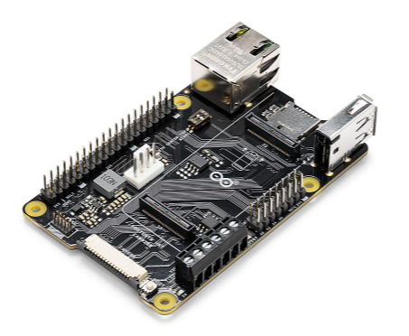
ASX00049

Arduino

* $43.32 - * $50.39

IN STOCK 2847
Buy

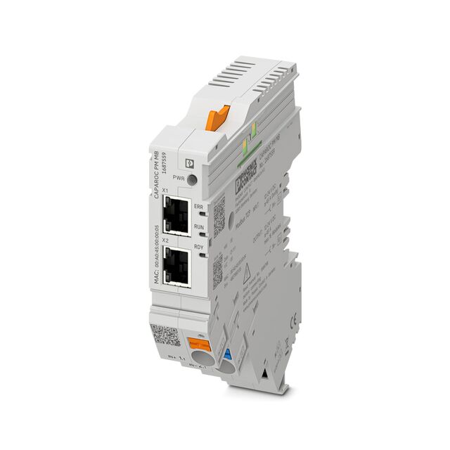
1687559

Phoenix Contact Ltd

[no prices available]

IN STOCK 2
Buy

Reference Designs

RD006

Wurth Elektronik

RD006 - 3 W Dual-output isolated auxiliary supply for communication interfaces and measurement systems

CN0583

Analog Devices Inc.

Multistandard Micropower Verified Smoke Detection System-on-Module

Technical Resources

EVALUATION KITS

EVAL-AD7124-8SDZ

Analog Devices Inc.

$0.00 - * $79.17

IN STOCK 792
Buy
View All