
DC1369A-A
Analog Devices Inc.The LTC2261-14/LTC2260-14/LTC2259-14 are sampling 14-bit A/D converters designed for digitizing high frequency, wide dynamic range signals. They are perfect for demanding communications applications with AC performance that includes 73.4dB SNR and 85dB spurious free dynamic range (SFDR). Ultralow jitter of 0.17psRMS allows undersampling of IF frequencies with excellent noise performance.DC specs include ?1LSB INL (typical), ?0.3LSB DNL (typical) and no missing codes over temperature. The transition noise is a low 1.2LSBRMS.The digital outputs can be either full-rate CMOS, doubledata rate CMOS, or double-data rate LVDS. A separate output power supply allows the CMOS output swing to range from 1.2V to 1.8V.The ENC+ and ENC? inputs may be driven differentially or single ended with a sine wave, PECL, LVDS, TTL or CMOS inputs. An optional clock duty cycle stabilizer allows high performance at full speed for a wide range of clock duty cycles. Bits LTC2261-12 12 LTC2261-14 14 Applications Communications Cellular Base Stations Software Defined Radios Portable Medical Imaging Multi-Channel Data Acquisition Nondestructive Testing

DC1369A-N
Analog Devices Inc.The LTC2262-12 is a sampling 12-bit A/D converter designed for digitizing high frequency, wide dynamic range signals. The LTC2262-12 is perfect for demanding communications applications with AC performance that includes 70.5dB SNR and 88dB spurious free dynamic range (SFDR). Ultralow jitter of 0.17psRMS allows undersampling of IF frequencies with excellent noise performance.DC specs include ?0.3LSB INL (typical), ?0.1LSB DNL (typical) and no missing codes over temperature. The transition noise is a low 0.3LSBRMS.The digital outputs can be either full rate CMOS, double data rate CMOS, or double data rate LVDS. A separate output power supply allows the CMOS output swing to range from 1.2V to 1.8V.The ENC+ and ENC? inputs may be driven differentially or single-ended with a sine wave, PECL, LVDS, TTL or CMOS inputs. An optional clock duty cycle stabilizer allows high performance at full speed for a wide range of clock duty cycles. Bits LTC2262-12 12 LTC2262-14 14 Applications Communications Cellular Base Stations Software Defined Radios Portable Medical Imaging Multi-Channel Data Acquisition Nondestructive Testing
DC1370A-A
Analog Devices Inc.The LTC2261-14/LTC2260-14/LTC2259-14 are sampling 14-bit A/D converters designed for digitizing high frequency, wide dynamic range signals. They are perfect for demanding communications applications with AC performance that includes 73.4dB SNR and 85dB spurious free dynamic range (SFDR). Ultralow jitter of 0.17psRMS allows undersampling of IF frequencies with excellent noise performance.DC specs include ?1LSB INL (typical), ?0.3LSB DNL (typical) and no missing codes over temperature. The transition noise is a low 1.2LSBRMS.The digital outputs can be either full-rate CMOS, doubledata rate CMOS, or double-data rate LVDS. A separate output power supply allows the CMOS output swing to range from 1.2V to 1.8V.The ENC+ and ENC? inputs may be driven differentially or single ended with a sine wave, PECL, LVDS, TTL or CMOS inputs. An optional clock duty cycle stabilizer allows high performance at full speed for a wide range of clock duty cycles. Bits LTC2261-12 12 LTC2261-14 14 Applications Communications Cellular Base Stations Software Defined Radios Portable Medical Imaging Multi-Channel Data Acquisition Nondestructive Testing

LT3470AEDDB Demo Board | (DFN) 4V ≤ VIN ≤ 36V, VOUT = 3.3V @ 250mA, Integrated Boost and Catch Diodes
Analog Devices Inc.Demonstration circuit 1382 is a 40V micropower DFN buck regulator featuring the LT3470A. The LT3470A has a higher peak switch current and improved start-up and dropout compared with the non-"A" version. The demo board is optimized for 3.3V output at up to 250mA load current for a steady state input voltage range of 4V to 36V. With its wide input voltage range, high efficiency internal power switch, extremely low dropout operation, hysteretic current-mode, integrated boost and catch diodes and tiny DFN package, the LT3470A is a very versatile and powerful IC for DC/DC converters that require extremely compact space, high efficiency and high input voltage.
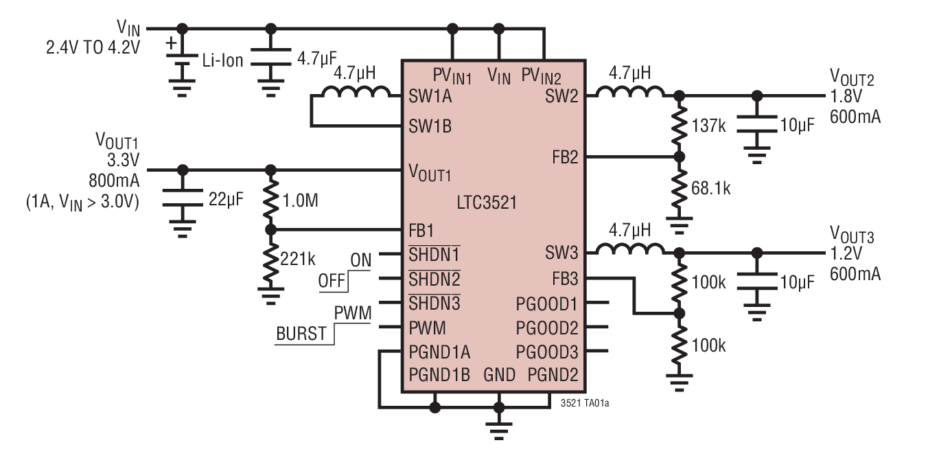
LTC3521EUF Demo Board | Buck-Boost Plus Dual Buck, 2.4V ≤ VIN ≤ 5V, VOUT1 = 3.3V @ 0.8A, VOUT2 = 1.2V @ 0.6A, VOUT3 = 1.8V @ 0.6A
Analog Devices Inc.Demonstration circuit 1389A is high efficiency triple output DC/DC power supply featuring the LTC3521. The IC includes a 4-switch synchronous Buck-Boost DC/DC converter with a 1A switch rating and two synchronous 600mA Buck converters. The demo board accepts an input voltage between 2.4V and 5V, and provides fixed output voltages of 3.3V @800mA for the Buck-Boost converter and 1.2V & 1.8V @600mA for the Buck converters.

LTC6802-2 (requires DC590B) New Designs Should Use DC1652 or DC1654 | Demo Board
Analog Devices Inc.DC1393B: Demo Board for LTC6802-2 Multicell Addressable Battery Stack Monitor

LT3505 HV Buck Regulator Board with Plug-in Interface
Analog Devices Inc.DC1395A: Demo Board for LT3505 1.2A, Step-Down Switching Regulator in 3mm × 3mm DFN

LTC4099EPDC Demo Board | I2C-Controlled USB Power Manager/Charger with Overvoltage Protection (requires DC590)
Analog Devices Inc.Demonstration Circuit 1396A is an I2C-controlled, high-efficiency USB/5V Powered 1A Li-Ion battery charger/manager with the control hooks for an external HV battery-tracking step-down controller (LT3480 is recommended). The Input current is automatically limited for USB compatibility. The DC1396's input voltage ranges from 4.35V to 5.5V, and the device provides overvoltage protection from up to 30V. The device features a CC/CV linear charger with a 4.2V charge voltage, C/x detection and timer termination.

LT3085EDCB Demo Board | Single Resistor, Low Dropout Regulator, 1.7V ≤ VIN ≤ 25V, VOUT = 1.2V/1.8V/2.5V/3.3V/5V/Adjustable @ 500mA
Analog Devices Inc.Demonstration circuit 1401A is an adjustable 500mA linear regulator featuring the LT3085. Architected as a precision current source and voltage follower, the LT3085 can be used in many applications requiring up to 500mA output current, adjustability down to 0V at the output and no heat sink. The device brings out the collector of the pass transistor to allow low dropout operation when used with multiple supplies. The demo board operates with an input voltage range from 1.7V to 25V (the maximum output voltage is limited by the output capacitor's voltage rating) and provides a jumper-selectable output voltage of 1.2V, 1.8V, 2.5V, 3.3V, 5V or a user-defined value.
For the LT3085 to regulate properly, the voltage on the control pin (VCONTROL) must be more than approximately 1.2V greater than the output voltage.

DC1410A-B
Analog Devices Inc.The LTC2444/LTC2445/LTC2448/LTC2449 are 8-/16- channel (4-/8-differential) high speed 24-bit No Latency ?? ADCs. They use a proprietary delta-sigma architecture enabling variable speed/resolution. Through a simple 4-wire serial interface, ten speed/resolution combinations 6.9Hz/280nVRMS to 3.5kHz/25?VRMS (4kHz with external oscillator) can be selected with no latency between conversion results or shift in DC accuracy (offset, full-scale, linearity, drift). Additionally, a 2X speed mode can be selected enabling output rates up to 7kHz (8kHz if an external oscillator is used) with one cycle latency.Any combination of single-ended or differential inputs can be selected with a common mode input range from ground to VCC, independent of VREF. While operating in the 1X speed mode the first conversion following a new speed, resolution, or channel selection is valid. Since there is no settling time between conversions, all 8 differential channels can be scanned at a rate of 500Hz. At the conclusion of each conversion, the converter is internally reset eliminating any memory effects between successive conversions and assuring stability of the high order delta-sigma modulator.Applications High Speed Multiplexing Weight Scales Auto Ranging 6-Digit DVMs Direct Temperature Measurement High Speed Data Acquisition

LTC3787EUFD Demo Board | 5V to 24VIN to 24VOUT at 6A
Analog Devices Inc.Demonstration circuit DC1411 is DC/DC boost converter featuring the LTC3787 constant frequency current mode boost controller. The DC1411A operates over 5V to 24V input and provides 6A to 16A of output current. The 350kHz constant frequency operation results in small and efficient circuit. The converter provides high output voltage accuracy (typically ±3%) over wide load range with no minimum load requirement. The demonstration circuit can be easily modified to generate different output voltages.

LT1222CS8 Demo Board | 500mHz, 3nV√Hz Operational Amplifier
Analog Devices Inc.DC1416B: Demo Board for the LT1222 500MHz, 3nV√Hz, AV ≥ 10 Operational Amplifier.
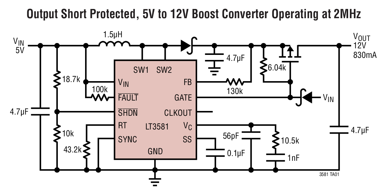
LT3581EMSE Demo Board | VIN = 5V to 10V, VOUT1 = 12V @ 900mA
Analog Devices Inc.Demonstration circuits 1424A-A and 1424A-B feature the LT3581 in Boost and Inverting Regulator configurations, respectively. The Boost is designed to convert a 5V to 10V input source to 12V at 900mA, and the Inverter a 5V to 12V to -12V at 750mA. DC1424A-A is designed to survive output short circuit events with the external MOSFET installed at the output as default. The demo board includes an option to install the MOSFET at the input side. Install Q1 and R1 on the back of the board and refer to Figure 4 for other instructions. DC1424A-B can easily be converted into a SEPIC Converter by swapping L2 and D2 from their respective locations as shown in Figure 5. The LT3581 includes a 42V Master and Slave switch combination with 3.3A total current and can be used in many configurations such as Boost, SEPIC, CUK and Flyback.
LT3581EMSE Demo Board | VIN = 5V to 12V, VOUT1 = –12V @ 750mA
Analog Devices Inc.Demonstration circuits 1424A-A and 1424A-B feature the LT3581 in Boost and Inverting Regulator configurations, respectively. The Boost is designed to convert a 5V to 10V input source to 12V at 900mA, and the Inverter a 5V to 12V to -12V at 750mA. DC1424A-A is designed to survive output short circuit events with the external MOSFET installed at the output as default. The demo board includes an option to install the MOSFET at the input side. Install Q1 and R1 on the back of the board and refer to Figure 4 for other instructions. DC1424A-B can easily be converted into a SEPIC Converter by swapping L2 and D2 from their respective locations as shown in Figure 5. The LT3581 includes a 42V Master and Slave switch combination with 3.3A total current and can be used in many configurations such as Boost, SEPIC, CUK and Flyback. It has a 2.5V to 22V operating input range, UVLO, soft-start, programmable switching frequency and many other popular features.

LTC3859A Demo Board | Triple Output, Buck/Buck/Boost, 4.5V ≤ VIN ≤ 36V, VOUT1 = 5V @ 5A, VOUT2 = 8.5V @ 3A, VOUT3 = 10V @ 2A
Analog Devices Inc.Demonstration circuit DC1425A is a triple output synchronous step-up/dual step-down power supply featuring the LTC3859AIFE. The demo board is has the LTC3859AIFE buck inputs supplied from the boost output. With this boost-then-buck topology, the buck outputs maintain regulation over the entire 4.5V to 36V input range and the application is suitable for automotive or other battery fed applications where low quiescent current is important. The buck controllers provide 5V @ 5A and 8.5V @ 3A and the boost can supply 10V @ 2A when the bucks are drawing their maximim load current.

DC1431A-C
Analog Devices Inc.The LTC5542 is part of a family of high dynamic range, high gain, passive downconverting mixers covering the 600MHz to 4GHz frequency range. The LTC5542 is optimized for 1.6GHz to 2.7GHz RF applications. The LO frequency must fall within the 1.7GHz to 2.5GHz range for optimum performance. A typical application is a LTE or WiMAX receiver with a 2.3GHz to 2.7GHz RF input and low-side LO. The LTC5542 is designed for 3.3V operation, however; the IF amplifier can be powered by 5V for the highest P1dB. An integrated SPDT LO switch with fast switching accepts two active LO signals, while providing high isolation. The LTC5542?s high conversion gain and high dynamic range enable the use of lossy IF filters in high-selectivity receiver designs, while minimizing the total solution cost, board space and system-level variation.Applications Wireless Infrastructure Receivers (LTE, W-CDMA. TD-SCDMA, WiMAX, GSM1800) Point-to-Point Microwave Links High Dynamic Range Downmixer Applications

LTC3851AUED Demo Board with Adjustable ILIMIT | 4.5V ≤ VIN ≤ 14V, VOUT = 1.5V @ 15A
Analog Devices Inc.Demonstration circuit 1432A is a synchronous buck controller featuring the LTC3851AEUD/LTC3851AEUD-1. It operates with an input voltage from 4.5V to 14V and provides 1.5V at up to 15A at the output. The demo circuit is available in two versions. DC1432A-A is configured with LTC3851AEUD which provides ISET function, while the DC1432A-B is configured with LTC3851AEUD-1 which provides PGOOD function.

DC1434A
Analog Devices Inc.The LT3071 is a low voltage, UltraFast? transient response linear regulator. The device supplies up to 5A of output current with a typical dropout voltage of 85mV. A 0.01?F reference bypass capacitor decreases output voltage noise to 25?VRMS. The LT3071?s high bandwidth permits the use of low ESR ceramic capacitors, saving bulk capacitance and cost. The LT3071?s features make it ideal for high performance FPGAs, microprocessors or sensitive communication supply applications.Output voltage is digitally selectable in 50mV increments over a 0.8V to 1.8V range. An analog margining function allows the user to adjust system output voltage over a continuous ?10% range. The IC incorporates a unique tracking function to control a buck regulator powering the LT3071?s input. This tracking function drives the buck regulator to maintain the LT3071?s input voltage to VOUT + 300mV, minimizing power dissipation.Internal protection includes UVLO, reverse-current protection, precision current limiting with power foldback and thermal shutdown. The LT3071 regulator is available in a thermally enhanced 28-lead, 4mm ? 5mm QFN package.APPLICATIONS FPGA and DSP Supplies ASIC and Microprocessor Supplies Servers and Storage Devices Post Buck Regulation and Supply Isolation

LTC3615EUF Demo Board (QFN) | 2.25V ≤ VIN ≤ 5.5V, VOUT1 = 1.8V to 3.3V @ 3A, VOUT2 = 1.2V to 1.8V @ 3A
Analog Devices Inc.Demonstration circuit 1435 is a dual output regulator consisting of two constant-frequency step-down converters, based on the LTC3615 dual channel monolithic synchronous buck regulator in the 4mm × 4mm QFN-24 package. The DC1435 has an input voltage range of 2.25V to 5.5V, with each regulator capable of delivering up to 3A of output current. The DC1435 can operate in Burst Mode®, pulse-skip or forced continuous mode. In shutdown, the DC1435 requires less than 100 uA total. The DC1435 is a very efficient circuit: over 90% for either circuit. The LTC3615 comes in a 24 Pin QFN or leaded package, which each having an exposed pad on the bottom-side of the IC for better thermal performance.
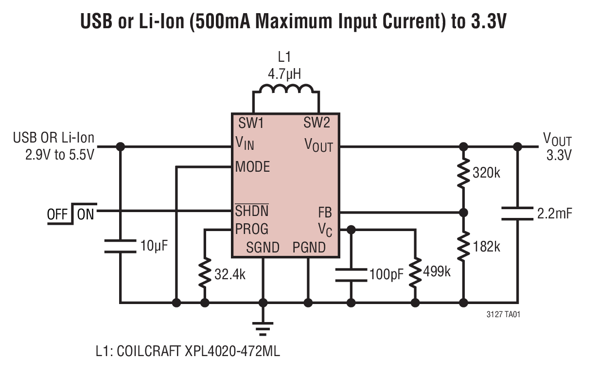
LTC3127EDD Demo Board | Programmable Average Input Current Limit, 1.2MHz, 1.8V ≤ VIN ≤ 5.5V, VOUT = 3.8V @ 2A Pulsed
Analog Devices Inc.Demonstration circuit 1451A is a Buck-Boost DC/DC converter featuring the LTC3127EDD and is ideally suited for pulsed load applications where the input current needs to be limited. Demonstration circuit 1451A is configured for 1.0A maximum input current limit and can handle pulsed load currents of up to 2A, with duty cycles of up to 15%. The input voltage range is 1.8V to 5.5V. The fixed input current limit can be adjusted by replacing one resistor (R6).


