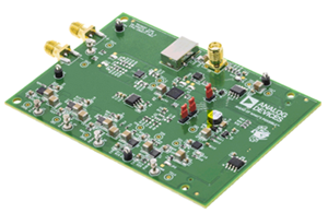
ADP7182CP-EVALZ
Analog Devices Inc.The ADP7182 is a CMOS, low dropout (LDO) linear regulator that operates from ?2.7 V to ?28 V and provides up to ?200 mA of output current. This high input voltage LDO is ideal for regulation of high performance analog and mixed signal circuits operating from ?27 V down to ?1.2 V rails. Using an advanced proprietary architecture, it provides high power supply rejection and low noise, and achieves excellent line and load transient response with a small 2.2 ?F ceramic output capacitor.The ADP7182 is available in fixed output voltage and an adjustable version that allows the output voltage to range from ?1.22 V to ?VIN + VDO via an external feedback divider.The following fixed output voltages are available from stock: ?5 V (3 mm ? 3 mm LFCSP), ?1.8 V, ?2.5 V, ?3 V, ?5 V (TSOT), ?1.2 V, ?1.5 V, ?2.5 V, ?5 V (2.00 mm ? 2.00 mm LFCSP). Additional voltages are available by special order.The ADP7182 regulator output noise is 18 ?V rms independent of the output voltage. The enable logic is capable of interfacing with positive or negative logic levels for maximum flexibility. The ADP7182 is available in 5-lead TSOT, 6- and 8-lead LFCSP packages for a small, low profile footprint.Applications Regulation to noise sensitive applications Analog-to-digital converter (ADC) and digital-to-analog converter (DAC) circuits, precision amplifiers Communications and infrastructure Medical and healthcare Industrial and instrumentation
ADP7182UJ-EVALZ
Analog Devices Inc.The ADP7182 is a CMOS, low dropout (LDO) linear regulator that operates from ?2.7 V to ?28 V and provides up to ?200 mA of output current. This high input voltage LDO is ideal for regulation of high performance analog and mixed signal circuits operating from ?27 V down to ?1.2 V rails. Using an advanced proprietary architecture, it provides high power supply rejection and low noise, and achieves excellent line and load transient response with a small 2.2 ?F ceramic output capacitor.The ADP7182 is available in fixed output voltage and an adjustable version that allows the output voltage to range from ?1.22 V to ?VIN + VDO via an external feedback divider.The following fixed output voltages are available from stock: ?5 V (3 mm ? 3 mm LFCSP), ?1.8 V, ?2.5 V, ?3 V, ?5 V (TSOT), ?1.2 V, ?1.5 V, ?2.5 V, ?5 V (2.00 mm ? 2.00 mm LFCSP). Additional voltages are available by special order.The ADP7182 regulator output noise is 18 ?V rms independent of the output voltage. The enable logic is capable of interfacing with positive or negative logic levels for maximum flexibility. The ADP7182 is available in 5-lead TSOT, 6- and 8-lead LFCSP packages for a small, low profile footprint.Applications Regulation to noise sensitive applications Analog-to-digital converter (ADC) and digital-to-analog converter (DAC) circuits, precision amplifiers Communications and infrastructure Medical and healthcare Industrial and instrumentation
ADP7185-3.3-EVALZ
Analog Devices Inc.The ADP7185 is a complementary metal oxide semiconductor(CMOS), low dropout (LDO) linear regulator that operatesfrom ?2.0 V to ?5.5 V and provides up to ?500 mA of output current. This high output current LDO is ideal for regulation of high performance analog and mixed signal circuits operatingfrom ?0.5 V down to ?4.5 V. Using an advanced proprietaryarchitecture, the ADP7185 provides high power supple rejectionratio (PSRR) and low noise, and it achieves excellent line and loadtransient response with a small 4.7 ?F ceramic output capacitor.The ADP7185 is available in 15 fixed output voltage options.The following voltages are available from stock: ?0.5 V, ?1.0 V,?1.2 V, ?1.5 V, ?1.8 V, ?2.0 V, ?2.5 V, ?3.0 V, and ?3.3 V.Additional voltages available by special order are ?0.8 V, ?0.9 V, ?1.3 V, ?2.8 V, ?4.2 V, and ?4.5 V. An adjustable version is also available which allows output voltages that range from ?0.5 V to ?VIN + 0.5 V with an external feedback divider.The enable logic feature is capable of interfacing with positive or negative logic levels for maximum flexibility.The ADP7185 regulator output noise is 4 ?V rms independent of the output voltage. The ADP7185 is available in an 8-lead, 2 mm ? 2 mm LFCSP, making it not only a very compact solution but also providing excellent thermal performance for applications requiring up to ?500 mA of output current in a small, low profile footprint.Applications Regulation to noise sensitive applications: analog-to-digital converters (ADCs), digital-to-analog converters (DACs), precision amplifiers Communications and infrastructure Medical and healthcare Industrial and instrumentation
Evaluating the ADP8860 Charge Pump, 7-Channel Smart LED Driver with I2C Interface
Analog Devices Inc.The ADP8860SHIELD-EVALZ and the ADP8861SHIELD-EVALZ incorporate light emitting diodes (LEDs) for quick and easy evaluation of the ADP8860 and the ADP8861. Note that only the ADP8860SHIELD-EVALZ has dual light intensity sensors. The ADP8860SHIELD-EVALZ and the ADP8861SHIELD-EVALZ follow the form factor of a regular Arduino® shield to allow compatibility with microcontroller boards that use the same interface. These evaluation boards also incorporate a separate header dedicated to I2C communications.
The ADP8860 and the ADP8861 are 7-channel LED drivers that utilizes a charge pump with selective gain for maximum efficiency. The LEDs driven by either device are programmable for maximum current and fade in and out times via the I2C interface. Only the ADP8860 has a programable light intensity threshold that can be set via the I2C interface of the device. Each channel can handle up to 30 mA (typical), except for the seventh channel, which can handle 60 mA (typical). Each channel can be unified to have the same fade in time and fade out time, or each channel can have an individual fade in time and fade out time for greater flexibility.
For full details on the ADP8860 and the ADP8861, see the ADP8860 and the ADP8861 data sheets, which should be consulted in conjunction with the user guide when using these evaluation boards.
ADPA7002-EVALZ
Analog Devices Inc.The ADPA7002CHIP is a gallium arsenide (GaAs), monolithic microwave integrated circuit (MMIC), pseudomorphic high electron mobility transistor (pHEMT), distributed power amplifier that operates from 20 GHz to 44 GHz. The amplifier provides 15 dB of small signal gain, 28 dBm output power at 1 dB gain compression (P1dB), and a typical output third-order intercept (IP3) of 40 dBm. The amplifier requires 600 mA from a 5 V supply on VDD2A, VDD2B, and VDD1. The ADPA7002CHIP also features inputs/outputs (I/Os) that are internally matched to 50 ?, and facilitates integration into multichip modules (MCMs). All data is taken with the on substrate chip connected via two wire bonds that are 0.025 mm (1 mil) wide and 0.31 mm (12 mils) long.Applications Military and space Test instrumentation
ADR1000H-EBZ
Analog Devices Inc.The ADR1000 is a 6.62 V, output highly stable, oven-controlled, buried Zener reference component built on an Analog Devices, Inc., proprietary bipolar process and is a pin-compatible replacement for the LTZ1000. Included on the chip is a buried Zener reference, a heater resistor for temperature stabilization, and a temperature sensing transistor. External circuitry is used to set the operating currents and the temperature of the reference, allowing the maximum flexibility to achieve maximum long-term stability and minimum noise.The ADR1000 application circuit can achieve a temperature coefficient of
ADR1399E-EBZ
Analog Devices Inc.The ADR1399 precision shunt reference features excellent temperature stability over a wide range of voltage, temperature, and quiescent current conditions. A temperature stabilizing loop is incorporated with the active Zener on a monolithic? substrate, which nearly eliminates changes in voltage with temperature. The subsurface Zener circuit is fully specified at a quiescent current IREF of 3 mA and offers minimal noise (1.44 ?V p-p, 0.1 Hz to 10 Hz) and excellent long-term stability (7 ppm/?kHr). The ADR1399 offers a lower output dynamic impedance (0.08 ?) than the LM399, reducing the effects of shunt resistor (RSHUNT) and the supply voltage variation on the reference output.Ideal applications for the ADR1399 include ultrastable digital voltmeters, precision calibration equipment, and ultrarepeatable analog-to-digital converters (ADCs). The simplicity of the basic pin configurations is shown in Figure 1. The 8-terminal LCC version offers force and sense pins for lower dynamic impedance and for Kelvin sensing. Table 1. Related Products Model Output Voltage (V) Initial Accuracy Range (mV) ADR1399 7.05 ?300 to +250 LTZ1000 7.2 ?200 to +300 LM399 6.95 ?200 to +350 LT1236 5 and 10 ?2.5 to +2.5 APPLICATIONS Precision voltage reference for multimeters Calibration equipment voltage standards Laboratory measurement equipment Industrial monitor and control instrumentation Ultrastable data convertors
ADRF5026-EVALZ-292
Analog Devices Inc.The ADRF5026 is a nonreflective, single-pole, double-throw (SPDT) radio frequency (RF) switch manufactured in a silicon process.The ADRF5026 operates from 100 MHz to 44 GHz with better than 3.8 dB of insertion loss and 45 dB of isolation. The ADRF5026 features an all off control, where both RF ports are in an isolation state. The ADRF5026 has a nonreflective design and both of the RF ports are internally terminated to 50 ?. The ADRF5026 requires a dual-supply voltage of +3.3 V and ?3.3 V. The device employs complimentary metal-oxide semiconductor/low-voltage transistor-transistor logic (CMOS/LVTTL) logic-compatible controls.The ADRF5026 is pin-compatible with the ADRF5027 low frequency cutoff version, which operates from 9 kHz to 44 GHz. The ADRF5026 RF ports are designed to match a characteristic impedance of 50 ?. For ultrawideband products, impedance matching on the RF transmission lines can further optimize high frequency insertion loss and return loss characteristics. Refer to the Narrow-Band Impedance Matching section for an example of a matched circuit that achieves a flat insertion loss response of 2.4 dB from 28 GHz to 43 GHz.The ADRF5026 comes in a 20-terminal, 3 mm ? 3 mm, RoHS-compliant, land grid array (LGA) package and can operate from ?40?C to +105?C.The ADRF5026 supports defense and aerospace applications (AQEC).Applications Industrial scanners Test and instrumentation Cellular infrastructure: 5G mmWave Military radios, radars, electronic counter measures (ECMs) Microwave radios and very small aperture terminals (VSATs)
ADRF5046-EVALZ
Analog Devices Inc.The ADRF5046 is a reflective, single-pole four-throw (SP4T) switch manufactured in the silicon process.?The ADRF5046 operates from 100 MHz to 44 GHz with insertion loss of lower than 3.0 dB and isolation of higher than 31 dB. The device has a radio frequency (RF) input power handling capability of 27 dBm for both the through path and hot switching.?The ADRF5046 draws a low current of 3 ?A on the positive supply of +3.3 V, and ?110 ?A on the negative supply of ?3.3 V.??The device provides complementary metal-oxide semiconductor (CMOS)-/low voltage transistor-transistor logic (LVTTL)-compatible controls.?The ADRF5046 comes in a 20-terminal, 3 mm ? 3 mm, RoHScompliant, land grid array (LGA) package and can operate from ?40?C to +105?C.?Applications Industrial Scanner Test and instrumentation Cellular Infrastructure ? mmWave 5G Military radios, radars, electronic counter measures (ECMs) Microwave radios and very small aperture terminals (VSATs)
ADRF5721-EVALZ
Analog Devices Inc.The ADRF5721 is a silicon, 4-bit digital attenuator with a 30 dB attenuation control range in 2 dB steps.This device operates from 9 kHz to 40 GHz with better than 3.4 dB of insertion loss. The ATTIN port of the ADRF5721 has a radio frequency (RF) input power handling capability of 26 dBm average and 30 dBm peak for all states.The ADRF5721 requires a dual supply voltage of +3.3 V and ?3.3 V. The device features serial peripheral interface (SPI), parallel mode control, and complementary metal-oxide semiconductor (CMOS)-/low voltage transistor to transistor logic (LVTTL)-compatible controls.The ADRF5721 is pin compatible with the ADRF5731, the fast switching version, which operates from 100 MHz to 40 GHz.The ADRF5721 RF ports are designed to match a characteristic impedance of 50 ?.The ADRF5721 comes in a 16-terminal, 2.5 mm ? 2.5 mm, RoHS compliant, land grid array (LGA) package and operates from ?40?C to +105?C.Applications Industrial scanners Test and instrumentation Cellular infrastructure: 5G millimeter wave Military radios, radars, electronic counter measures (ECMs) Microwave radios and very small aperture terminals (VSATs)
ADRF5730-EVALZ
Analog Devices Inc.The ADRF5730 is a silicon, 6-bit digital attenuator with 31.5 dB attenuation control range in 0.5 dB steps.This device operates from 100 MHz to 40 GHz with better than 4.8 dB of insertion loss and excellent attenuation accuracy. The ADRF5730 has a radio frequency (RF) input power handling capability of 27 dBm average and 30 dBm peak for all states.The ADRF5730 requires a dual supply voltage of +3.3 V and ?3.3 V. The device features serial peripheral interface (SPI), parallel mode control, and complementary metal-oxide semiconductor (CMOS)-/low voltage transistor to transistor logic (LVTTL)-compatible controls.The ADRF5730 is pin-compatible with the ADRF5720 low frequency cutoff version, which operates from 9 kHz to 40 GHz.The ADRF5730 RF ports are designed to match a characteristic impedance of 50 ?. For wideband applications, impedance matching on the RF transmission lines can further optimize high frequency insertion loss, return loss, and attenuation accuracy characteristics. Refer to the Electrical Specifications section, the Typical Performance Characteristics section, and the Applications Information section for more details.The ADRF5730 comes in a 24-terminal, 4 mm ? 4 mm, RoHS-compliant, land grid array (LGA) package and operates from ?40?C to +105?C.Applications Industrial scanners Test and instrumentation Cellular infrastructure: 5G millimeter wave Military radios, radars, electronic counter measures (ECMs) Microwave radios and very small aperture terminals (VSATs)
ADRF5740-EVALZ-185
Analog Devices Inc.The ADRF5740 is a silicon, 4-bit digital attenuator with 22 dB attenuation control range in 2 dB steps.The ADRF5740 operates from 10 MHz to 60 GHz with less than 3.3 dB of insertion loss and with ?(0.2 + 7.0% of attenuation state) of attenuation accuracy at 55 GHz. The ATTIN port of the ADRF5740 has an RF input power handling capability of 24 dBm average and 24 dBm peak for all states.The ADRF5740 requires a dual supply voltage of +3.3 V and ?3.3 V. The ADRF5740 features parallel mode control, and CMOS- and low voltage transistor to transistor logic (LVTTL)-compatible controls.The ADRF5740 RF ports are designed to match a characteristic impedance of 50 ?. The ADRF5740 comes in a 16-terminal, 2.5 mm ? 2.5 mm, RoHS compliant, land grid array (LGA) package and operates from ?40?C to +105?C.Applications Industrial scanners Test and instrumentation Cellular infrastructure: 5G millimeter wave Military radios, radars, electronic counter measures (ECMs) Microwave radios and very small aperture terminals (VSATs)
ADRV9002NP/W2/PCBZ
Analog Devices Inc.The ADRV9002 is a highly integrated RF transceiver that has dual-channel transmitters, dual-channel receivers, integrated synthesizers, and digital signal processing functions.The ADRV9002 is a high performance, highly linear, high dynamic range transceiver designed for performance vs. power consumption system optimization. The device is configurable and ideally suited to demanding, low power, portable and battery powered equipment. The ADRV9002 operates from 30 MHz to 6000 MHz and covers the UHF, VHF, industrial, scientific, and medical (ISM) bands, and cellular frequency bands in narrow-band (kHz) and wideband operation up to 40 MHz. The ADRV9002 is capable of both TDD and FDD operation.The transceiver consists of direct conversion signal paths with state-of-the-art noise figure and linearity. Each complete receiver and transmitter subsystem includes dc offset correction, quadrature error correction (QEC), and programmable digital filters, which eliminate the need for these functions in the digital baseband. In addition, several auxiliary functions, such as auxiliary analog-to-digital converters (ADCs), auxiliary digital-to-analog converters (DACs), and general-purpose inputs/outputs (GPIOs), are integrated to provide additional monitoring and control capability.The fully integrated phase-locked loops (PLLs) provide high performance, low power, fractional-N frequency synthesis for the transmitter, receiver, and clock sections. Careful design and layout techniques provide the isolation required in high performance personal radio applications. All voltage controlled oscillator (VCO) and loop filter components are integrated to minimize the external component count. The local oscillators (LOs) have flexible configuration options and include fast lock modes.The transceiver includes low power sleep and monitor modes to save power and extend the battery life of portable devices while monitoring communications.The fully integrated, low power digital predistortion (DPD) is optimized for both narrow-band and wideband signals and enables linearization of high efficiency power amplifiers.The ADRV9002 core can be powered directly from 1.0 V, 1.3 V, and 1.8 V regulators and is controlled via a standard 4-wire serial port. Other voltage supplies are used to provide proper digital interface levels and to optimize the receiver, transmitter, and auxiliary converter performance.High data rate and low data rate interfaces are supported using configurable CMOS or low voltage differential signaling (LVDS) serial synchronous interface (SSI) choice.The ADRV9002 is packaged in a 12 mm ? 12 mm, 196-ball chip scale package ball grid array (CSP_BGA).APPLICATIONS Mission critical communications Very high frequency (VHF), ultrahigh frequency (UHF), and cellular to 6 GHz Time division duplexing (TDD) and frequency division duplexing (FDD) applications
ADRV9026-HB/PCBZ
Analog Devices Inc.The ADRV9026 is a highly integrated, radio frequency (RF) agile transceiver offering four independently controlled transmitters, dedicated observation receiver inputs for monitoring each transmitter channel, four independently controlled receivers, integrated synthesizers, and digital signal processing functions providing a complete transceiver solution. The device provides the performance demanded by cellular infrastructure applications, such as small cell base station radios, macro 3G/4G/5G systems, and massive multiple in/multiple out (MIMO) base stations. The receiver subsystem consists of four independent, wide bandwidth, direct conversion receivers with wide dynamic range. The four independent transmitters use a direct conversion modulator resulting in low noise operation with low power consumption. The device also includes two wide bandwidth, time shared, observation path receivers with two inputs each for monitoring transmitter outputs. The complete transceiver subsystem includes automatic and manual attenuation control, dc offset correction, quadrature error correction (QEC), and digital filtering, eliminating the need for these functions in the digital baseband. Other auxiliary functions such as analog-to-digital converters (ADCs), digital-to-analog converters (DACs), and general-purpose input/outputs (GPIOs) that provide an array of digital control options are also integrated. To achieve a high level of RF performance, the transceiver includes five fully integrated phase-locked loops (PLLs). Two PLLs provide low noise and low power fractional-N RF synthesis for the transmitter and receiver signal paths. A third fully integrated PLL supports an independent local oscillator (LO) mode for the observation receiver. The fourth PLL generates the clocks needed for the converters and digital circuits, and a fifth PLL provides the clock for the serial data interface. A multichip synchronization mechanism synchronizes the phase of all LOs and baseband clocks between multiple ADRV9026 chips. All voltage controlled oscillators (VCOs) and loop filter components are integrated and adjustable through the digital control interface. The serial data interface consists of four serializer lanes and four deserializer lanes. The interface supports both the JESD204B and JESD204C standards, operating at data rates up to 24.33 Gbps. The interface also supports interleaved mode for lower bandwidths, thus reducing the number of high speed data interface lanes to one. Both fixed and floating-point data formats are supported. The floating-point format allows internal automatic gain control (AGC) to be invisible to the demodulator device. The ADRV9026 is powered directly from 1.0 V, 1.3 V, and 1.8 V regulators and is controlled via a standard serial peripheral interface (SPI) serial port. Comprehensive power-down modes are included to minimize power consumption in normal use. The ADRV9026 is packaged in a 14 mm ? 14 mm, 289-ball chip scale ball grid array (CSP_BGA).Applications 3G/4G/5G TDD and FDD massive MIMO, macro and small cell base stations
ADRV9375-N/PCBZ
Analog Devices Inc.The AD9375 is a highly integrated, wideband radio frequency (RF) transceiver offering dual-channel transmitters (Tx) and receivers (Rx), integrated synthesizers, a fully integrated digital predistortion (DPD) actuator and adaptation engine, and digital signal processing functions. The IC delivers a versatile combination of high performance and low power consumption required by 3G/4G small cell and massive multiple input, multiple output (MIMO) equipment in both frequency division duplex (FDD) and time division duplex (TDD) applications. The AD9375 operates from 300 MHz to 6000 MHz, covering most of the licensed and unlicensed cellular bands. The DPD algorithm supports linearization on signal bandwidths up to 40 MHz depending on the power amplifier (PA) characteristics (for example, two adjacent 20 MHz carriers). The IC supports Rx bandwidths up to 100 MHz. It also supports observation receiver (ORx) and Tx synthesis bandwidths up to 250 MHz to accommodate digital correction algorithms.The transceiver consists of wideband direct conversion signal paths with state-of-the-art noise figure and linearity. Each complete Rx and Tx subsystem includes dc offset correction, quadrature error correction (QEC), and programmable digital filters, eliminating the need for these functions in the digital baseband. Several auxiliary functions such as an auxiliary analog-to-digital converter (ADC), auxiliary digital-to-analog converters (DACs), and general-purpose input/outputs (GPIOs) are integrated to provide additional monitoring and control capability.An ORx channel with two inputs is included to monitor each Tx output and implement calibration applications. This channel also connects to three sniffer receiver (SnRx) inputs that can monitor radio activity in different bands.The high speed JESD204B interface supports lane rates up to 6144 Mbps. Four lanes are dedicated to the transmitters and four lanes are dedicated to the receiver and observation receiver channels.The fully integrated phase-locked loops (PLLs) provide high performance, low power, fractional-N frequency synthesis for the Tx, the Rx, the ORx, and the clock sections. Careful design and layout techniques provide the isolation demanded in high performance base station applications. All voltage controlled oscillator (VCO) and loop filter components are integrated to minimize the external component count.The device contains a fully integrated, low power DPD actuator and adaptation engine for use in PA linearization. The DPD feature enables use of high efficiency PAs, significantly reducing the power consumption of small cell base station radios while also reducing the number of JESD204B lanes necessary to interface with baseband processors.A 1.3 V supply is required to power the AD9375 core, and a standard 4-wire serial port controls it. Other voltage supplies provide proper digital interface levels and optimize transmitter and auxiliary converter performance. The AD9375 is packaged in a 12 mm ? 12 mm, 196-ball chip scale ball grid array (CSP_BGA).Applications 3G/4G small cell base stations (BTS) 3G/4G massive MIMO/active antenna systems
ADRV9375-W/PCBZ
Analog Devices Inc.The AD9375 is a highly integrated, wideband radio frequency (RF) transceiver offering dual-channel transmitters (Tx) and receivers (Rx), integrated synthesizers, a fully integrated digital predistortion (DPD) actuator and adaptation engine, and digital signal processing functions. The IC delivers a versatile combination of high performance and low power consumption required by 3G/4G small cell and massive multiple input, multiple output (MIMO) equipment in both frequency division duplex (FDD) and time division duplex (TDD) applications. The AD9375 operates from 300 MHz to 6000 MHz, covering most of the licensed and unlicensed cellular bands. The DPD algorithm supports linearization on signal bandwidths up to 40 MHz depending on the power amplifier (PA) characteristics (for example, two adjacent 20 MHz carriers). The IC supports Rx bandwidths up to 100 MHz. It also supports observation receiver (ORx) and Tx synthesis bandwidths up to 250 MHz to accommodate digital correction algorithms.The transceiver consists of wideband direct conversion signal paths with state-of-the-art noise figure and linearity. Each complete Rx and Tx subsystem includes dc offset correction, quadrature error correction (QEC), and programmable digital filters, eliminating the need for these functions in the digital baseband. Several auxiliary functions such as an auxiliary analog-to-digital converter (ADC), auxiliary digital-to-analog converters (DACs), and general-purpose input/outputs (GPIOs) are integrated to provide additional monitoring and control capability.An ORx channel with two inputs is included to monitor each Tx output and implement calibration applications. This channel also connects to three sniffer receiver (SnRx) inputs that can monitor radio activity in different bands.The high speed JESD204B interface supports lane rates up to 6144 Mbps. Four lanes are dedicated to the transmitters and four lanes are dedicated to the receiver and observation receiver channels.The fully integrated phase-locked loops (PLLs) provide high performance, low power, fractional-N frequency synthesis for the Tx, the Rx, the ORx, and the clock sections. Careful design and layout techniques provide the isolation demanded in high performance base station applications. All voltage controlled oscillator (VCO) and loop filter components are integrated to minimize the external component count.The device contains a fully integrated, low power DPD actuator and adaptation engine for use in PA linearization. The DPD feature enables use of high efficiency PAs, significantly reducing the power consumption of small cell base station radios while also reducing the number of JESD204B lanes necessary to interface with baseband processors.A 1.3 V supply is required to power the AD9375 core, and a standard 4-wire serial port controls it. Other voltage supplies provide proper digital interface levels and optimize transmitter and auxiliary converter performance. The AD9375 is packaged in a 12 mm ? 12 mm, 196-ball chip scale ball grid array (CSP_BGA).Applications 3G/4G small cell base stations (BTS) 3G/4G massive MIMO/active antenna systems
ADRV-DPD1/PCBZ
Analog Devices Inc.The AD9375 is a highly integrated, wideband radio frequency (RF) transceiver offering dual-channel transmitters (Tx) and receivers (Rx), integrated synthesizers, a fully integrated digital predistortion (DPD) actuator and adaptation engine, and digital signal processing functions. The IC delivers a versatile combination of high performance and low power consumption required by 3G/4G small cell and massive multiple input, multiple output (MIMO) equipment in both frequency division duplex (FDD) and time division duplex (TDD) applications. The AD9375 operates from 300 MHz to 6000 MHz, covering most of the licensed and unlicensed cellular bands. The DPD algorithm supports linearization on signal bandwidths up to 40 MHz depending on the power amplifier (PA) characteristics (for example, two adjacent 20 MHz carriers). The IC supports Rx bandwidths up to 100 MHz. It also supports observation receiver (ORx) and Tx synthesis bandwidths up to 250 MHz to accommodate digital correction algorithms.The transceiver consists of wideband direct conversion signal paths with state-of-the-art noise figure and linearity. Each complete Rx and Tx subsystem includes dc offset correction, quadrature error correction (QEC), and programmable digital filters, eliminating the need for these functions in the digital baseband. Several auxiliary functions such as an auxiliary analog-to-digital converter (ADC), auxiliary digital-to-analog converters (DACs), and general-purpose input/outputs (GPIOs) are integrated to provide additional monitoring and control capability.An ORx channel with two inputs is included to monitor each Tx output and implement calibration applications. This channel also connects to three sniffer receiver (SnRx) inputs that can monitor radio activity in different bands.The high speed JESD204B interface supports lane rates up to 6144 Mbps. Four lanes are dedicated to the transmitters and four lanes are dedicated to the receiver and observation receiver channels.The fully integrated phase-locked loops (PLLs) provide high performance, low power, fractional-N frequency synthesis for the Tx, the Rx, the ORx, and the clock sections. Careful design and layout techniques provide the isolation demanded in high performance base station applications. All voltage controlled oscillator (VCO) and loop filter components are integrated to minimize the external component count.The device contains a fully integrated, low power DPD actuator and adaptation engine for use in PA linearization. The DPD feature enables use of high efficiency PAs, significantly reducing the power consumption of small cell base station radios while also reducing the number of JESD204B lanes necessary to interface with baseband processors.A 1.3 V supply is required to power the AD9375 core, and a standard 4-wire serial port controls it. Other voltage supplies provide proper digital interface levels and optimize transmitter and auxiliary converter performance. The AD9375 is packaged in a 12 mm ? 12 mm, 196-ball chip scale ball grid array (CSP_BGA).Applications 3G/4G small cell base stations (BTS) 3G/4G massive MIMO/active antenna systems
ADV3202-EVALZ
Analog Devices Inc.The ADV3202/ADV3203 are 32 ? 16 analog crosspoint switch matrices. They feature a selectable sync-tip clamp input forac-coupled applications and a 2:1 on-screen display (OSD) insertion mux. With ?48 dB of crosstalk and ?80 dB isolationat 5 MHz, the ADV3202/ADV3203 are useful in many high density routing applications. The 0.1 dB flatness out to 60 MHz makes the ADV3202/ADV3203 ideal for both composite and component video switching.The 16 independent output buffers of the ADV3202/ADV3203 can be placed into a high impedance state for paralleling crosspoint outputs so that off-channels present minimal loading to an output bus if building a larger array. The ADV3202 has a gain of +1 while the ADV3203 has a gain of +2 for ease of use in back-terminated load applications. A single +5 V supply, dual ?2.5 V supplies, or dual ?3.3 V supplies can be used while consuming only 195 mA of idle current with all outputs enabled. The channel switching is performed via a double buffered, serial digital control, that can accommodate daisy chaining of several devices.The ADV3202/ADV3203 are packaged in a 176-lead exposed pad LQFP package (24 mm ? 24 mm) and are available over the extended industrial temperature range of ?40?C to +85?C.Applications CCTV surveillance Routing of high speed signals ? ? ? Composite video (NTSC, PAL, S, SECAM) ? ? ? RGB and component video routing ? ? ? Compressed video (MPEG, wavelet) Video conferencingData Sheet, Rev 0, 11/2008
ADV3224-EVALZ
Analog Devices Inc.The ADV3224/ADV3225 are high speed 16 ? 8 analog crosspoint switch matrices. They offer a ?3 dB signal bandwidth of greater than 750 MHz and a high slew rate of greater than 2500 V/?s.The ADV3224/ADV3225 include eight independent output buffers that can be placed into a high impedance state for paralleling crosspoint outputs to prevent off channels from loading the output bus. The ADV3224 has a gain of +1 and the ADV3225 has a gain of +2, and they both operate on voltage supplies of ?5 V. Channel switching is performed via a serial digital control that can accommodate the daisy chaining of several devices or via a parallel control to allow updating of an individual output without reprogramming the entire array.The ADV3224/ADV3225 are available in the 72-lead LFCSP package over the extended industrial temperature range of ?40?C to +85?C.Applications Routing of high speed signals including Video (NTSC, PAL, S, SECAM, YUV, RGB) Compressed video (MPEG, wavelet) 3-level digital video (HDB3) Data communications Telecommunications
ADV3229-EVALZ
Analog Devices Inc.The ADV3228/ADV3229 are high speed 8 ? 8 analog crosspoint switch matrices. They offer a ?3 dB large signal bandwidth of 750 MHz (ADV3228) and a slew rate of 2500 V/?s.The ADV3228/ADV3229 include eight independent output buffers that can be placed into a high impedance state for paralleling crosspoint outputs to prevent off channels from loading the output bus. The ADV3228 has a gain of +1, the ADV3229 has a gain of +2, and they both operate on voltage supplies of ?5 V. Channel switching is performed via a serial digital control that can accommodate daisy chaining of several devices or via a parallel control to allow updating of an individual output without reprogramming the entire array.The ADV3228/ADV3229 are available in the 72-lead LFCSP package over the extended industrial temperature range of ?40?C to +85?C.Applications Routing of high speed signals including: Video (NTSC, PAL, S, SECAM, YUV, RGB) Compressed video (MPEG, wavelet) 3-level digital video (HDB3) Data communications Telecommunications


