Top Manufacturers
Stock

Displaying 4141 - 4160 of 5453

Evaluation Kits from Analog Devices Inc.

EV1HMC8413LP2F

Analog Devices Inc.
The HMC8413 is a gallium arsenide (GaAs), monolithic microwave integrated circuit (MMIC), pseudomorphic high electron mobility transistor (pHEMT), low noise wideband amplifier that operates from 0.01 GHz to 9 GHz.The HMC8413 provides a typical gain of 19.5 dB, a 1.9 dB typical noise figure, and a typical output third-order intercept (OIP3) of 35 dBm at 0.01 GHz to 7 GHz, requiring only 95 mA from a 5 V supply voltage. The saturated output power (PSAT) of 22 dBm typical at 0.01 GHz to 7 GHz enables the low noise amplifier to function as a local oscillator (LO) driver for many of Analog Devices, Inc., balanced, in-phase/quadrature (I/Q) or image rejection mixers.The HMC8413 also features inputs and outputs that are internally matched to 50 ?, making the device ideal for surface-mounted technology (SMT)-based, high capacity microwave radio applications.The HMC8413 is housed in an RoHS-compliant, 2 mm ? 2 mm, 6-lead LFCSP.APPLICATIONS Test instrumentation Military communications Military radar Telecommunications

EV1HMC862ALP3

Analog Devices Inc.
The HMC862A is a low noise, programmable frequency divider in a 3 mm ? 3 mm, leadless, surface-mount package. The frequency divider, N, can be programmed to divide from 1, 2, 4, or 8 in the 0.1 GHz to 24 GHz input frequency range.The low phase noise, wide frequency range, and flexible division ratio make this device ideal for high performance and wideband communication systems.Applications Satellite communication systems Point to point and point to multipoint radios Military applications Test equipment

EV1HMC882ALP5

Analog Devices Inc.
The HMC882A is a monolithic microwave integrated circuit(MMIC) low-pass filter that features a user-selectable cutofffrequency (f3dB). The cutoff frequency can be varied from3.95 GHz to 6.9 GHz by applying a single analog tuning voltagebetween 0 V and 14 V. This low-pass filter provides a low 3 dBinsertion loss, 13 dB return loss, and >20 dB stopband attenuationat 1.28 ? f3dB GHz. This tunable filter can be used as a muchsmaller alternative to physically large switched filter banks andcavity tuned filters. The HMC882A has excellent microphonicsdue to the monolithic design and low residual phase noise of?165 dBc/Hz, and provides a dynamically adjustable solution inadvanced communications applications. The low-pass tunablefilter is packaged in a RoHS compliant, 5 mm ? 5mm LFCSPpackage.Applications Testing and measurement equipment Military radar and electronic warfare/electronic counter measures (ECMs) Satellite communication and space Industrial and medical equipment

EV1HMC943APM5

Analog Devices Inc.
The HMC943APM5E is a four stage, gallium arsenide (GaAs), pseudomorphic high electron mobility transistor (pHEMT), monolithic microwave integrated circuit (MMIC), >1.5 W power amplifier that operates between 24 GHz to 34 GHz. The HMC943APM5E provides 23 dB of gain, 34 dBm of saturated output power (PSAT), and 23% power added efficiency (PAE) from a 5.5 V supply. The high output third-order intercept (IP3) of 39 dBm makes the HMC943APM5E ideal for microwave radio applications. A power detector output is also available. The HMC943APM5E amplifier input/outputs (I/Os) are internally matched to 50 ?. The device is packaged in a leadless, 5 mm ? 5 mm, surface-mount LFCSP_CAV package, and requires no external matching components.Applications Point to point radios Point to multipoint radios Microwave radios, very small aperture terminals (VSATs), and satellite communications (SATCOM) Military and space

EV1HMC998APM5

Analog Devices Inc.
The HMC998APM5E is a GaAs pHEMT MMIC Distributed Power Amplifier which operates from DC to 22 GHz. The amplifier provides +15 dB of gain, +42 dBm output IP3, and +32 dBm of output power at 1dB gain compression while requiring only 500mA from a +15V supply. The HMC998APM5E exhibits a slightly positive gain slope from 3 to 17 GHz making it ideal for military and space and test equipment applications. The HMC998APM5E amplifier I/Os are internally matched to 50 Ohms and is housed ina RoHS compliant, 5x5 mm leadless QFN surface mount package.APPLICATIONS Test instumentation Military & space Fiber optics

EV2HMC6832ALP5L

Analog Devices Inc.
The HMC6832 is an input selectable, 2:8 differential fanoutbuffer designed for low noise clock distribution. The IN_SELcontrol pin selects one of the two differential inputs. This inputis then buffered to all eight differential outputs. The low jitteroutputs of the HMC6832 lead to synchronized low noiseswitching of downstream circuits, such as mixers, analog-todigitalconverters (ADCs)/digital-to-analog converters (DACs),or serializer/deserializer (SERDES) devices. The device is capableof low voltage, positive emitter-coupled logic (LVPECL) or lowvoltage differential signaling (LVDS) configurations by pullingthe CONFIG pin low for LVPECL or high or open (internallypulled high) for pseudo LVDS.Product Highlights Multiple Output Configurations. The CONFIG pin allows the user to select LVPECL or LVDS output termination. Multiple Supply Voltage Operation. The HMC6832 operates at 2.5 V or 3.3 V for LVPECL terminations (2.5 V only for LVDS). Low Noise. The HMC6832 noise is low, typically from ?168 dBc/Hz to ?162 dBc/Hz up to 3000 MHz. Low Propagation Delay. The HMC6832 displays a low delay, less than 207 ps, typical. Channel skew is also low, ?5 ps, typical. Low Core Current. The HMC6832 has a low core current of 56 mA, typical. Applications SONET, Fibre Channel, GigE clock distribution ADC/DAC clock distribution Low skew and jitter clocks Wireless/wired communications Level translation High performance instrumentation Medical imaging Single-ended to differential conversions

EV-AD4020-REF-DGNZ

Analog Devices Inc.
The AD4020 is a high accuracy, high speed, low power, 20-bit, Easy Drive, precision successive approximation register (SAR) analog-to-digital converter (ADC) that operates from a single power supply, VDD. The reference voltage, VREF, is applied externally and can be set independent of the supply voltage. The AD4020 power scales linearly with throughput.Easy Drive features reduce both signal chain complexity and power consumption while enabling higher channel density. The reduced input current, particularly in high-Z mode, coupled with a long signal acquisition phase, eliminates the need for a dedicated ADC driver. Easy Drive broadens the range of companion circuitry that is capable of driving these ADCs (see Figure 2 in the data sheet).Input span compression eliminates the need to provide a negative supply to the ADC driver amplifier while preserving access to the full ADC code range. The input overvoltage clamp protects the ADC inputs against overvoltage events, minimizing disturbances on the reference pin, and eliminating the need for external protection diodes.?Fast device throughput up to 1.8 MSPS allows users to accurately capture high frequency signals and to implement oversampling techniques to alleviate the challenges associated with antialias filter designs. Decreased serial peripheral interface (SPI) clock rate requirements reduce digital input/output power consumption, broadens digital host options, and simplifies the task of sending data across digital isolation. The SPI-compatible serial user interface is compatible with 1.8 V, 2.5 V, 3 V, and 5 V logic by using the separate VIO logic supply.APPLICATIONS Automatic test equipment Machine automation Medical equipment Battery-powered equipment Precision data acquisition systems Instrumentation and control systems

EV-AD5415/49SDZ

Analog Devices Inc.
The AD5415 is a CMOS, 12-bit, dual channel, current output digital-to-analog converter. This device operates from a 2.5 V to 5.5 V power supply, making it suited to battery-powered applications and other applications.As a result of being manufactured on a CMOS submicron process, this part offers excellent 4-quadrant multiplication characteristics, with large-signal multiplying bandwidths of 10 MHz.The applied external reference input voltage (VREF) determines the full scale output current. An integrated feedback resistor (RFB) provides temperature tracking and full scale voltage output when combined with an external current to voltage precision amplifier. In addition, this device contains the 4-quadrant resistors necessary for bipolar operation and other configuration modes.This DAC uses a double buffered, 3-wire serial interface that is compatible with SPI?, QSPI?, MICROWIRE?, and most DSP interface standards. In addition, a serial data out pin (SDO) allows daisy-chaining when multiple packages are used. Data readback allows the user to read the contents of the DAC register via the SDO pin. On power-up, the internal shift register and latches are filled with 0s, and the DAC outputs are at zero scale.The AD5415 DAC is available in a 24-lead TSSOP package. The EVAL-AD5415/AD5449SDZ evaluation board is available for evaluating DAC performance. For more information, see the UG-296 evaluation board user guide.APPLICATIONS Portable battery-powered applications Waveform generators Analog processing Instrumentation applications Programmable amplifiers and attenuators Digitally controlled calibration Programmable filters and oscillators Composite video Ultrasound Gain, offset, and voltage trimming

EV-AD5443/46/53SDZ

Analog Devices Inc.
The AD5426 / AD5432 / AD5443 EVAL-AD5443SDZ / EVAL-AD5446SDZ / EVAL-AD5453SDZ are CMOS 8-, 10-, and 12-bit current output digital-to-analog converters (DACs), respectively. These devices operate from a 2.5 V to 5.5 V power supply, making them suitable for battery-powered applications and many other applications.These DACs use a double buffered, 3-wire serial interface that is compatible with SPI, QSPI?, MICROWIRE?, and most DSP interface standards. In addition, a serial data out pin (SDO) allows for daisy-chaining when multiple packages are used. Data readback allows the user to read the contents of the DAC register via the SDO pin. On power-up, the internal shift register and latches are filled with 0s and the DAC outputs are at zero scale.As a result of manufacturing on a CMOS submicron process, the parts offer excellent 4-quadrant multiplication characteristics with large signal multiplying bandwidths of 10 MHz. The applied external reference input voltage, VREF, determines the full-scale output current. An integrated feedback resistor, RFB, provides temperature tracking and full-scale voltage output when combined with an external current to voltage precision amplifier.The AD5426 / AD5432 / AD5443 EVAL-AD5443SDZ / EVAL-AD5446SDZ / EVAL-AD5453SDZ DACs are available in small, 10-lead MSOP packages.The EVAL-AD5443SDZ / EVAL-AD5446SDZ / EVAL-AD5453SDZ evaluation board is available for evaluating DAC performance. For more information, see the UG-327 evaluation board user guide.APPLICATIONS Portable battery-powered applications Waveform generators Instrumentation Programmable amplifiers and attenuators Digitally controlled calibration Programmable filters and oscillators Composite video Ultrasound Gain, offset, and voltage trimming

EV-AD7284TMSDZ

Analog Devices Inc.
The AD7284 contains all the functions required for the general-purpose monitoring of stacked Li-Ion batteries, as used in hybrid electric vehicles and battery backup applications.The AD7284 has multiplexed cell voltage and auxiliary, analog-to-digital converter (ADC) measurement channels supporting four to eight cells of battery management. The device provides a maximum total unadjusted error, TUE, (cell voltage accuracy) of ?3 mV that includes all the internal errors from input to output. The primary ADC resolution is 14 bits.The AD7284 also includes an integrated secondary measurement path that validates the data on the primary ADC. Other diagnostic features include the detection of open inputs, communication, and power supply related faults.The AD7284 cell balancing interface outputs control the external field effect transistors (FETs) to allow discharging of individual cells.There are two on-chip 2.5 V voltage references: one reference for the primary measurement path, and one for the secondary measurement path.The AD7284 operates from one VDD supply, ranging from 10 V to 40 V. The device provides eight differential analog input channels to accommodate large common-mode signals across the full VDD range. Each channel allows an input signal range, VPINx ? VPIN(x ? 1) and VSINx ? VSIN(x ? 1), of 0 V to 5 V, where x = 0 to 8. The input pins assume a series stack of eight cells. The AD7284 includes four auxiliary ADC input channels that can be used for temperature measurement or system diagnostics.The AD7284 has a differential daisy-chain interface that allows multiple devices to be stacked without the need for individual device isolation. By design, this interface allows both device to device communication within the same module and communication between devices on different modules.Applications Li-Ion battery monitoring Electric and hybrid electric vehicles Stationary power applications

EV-AD7768-1FMCZ

Analog Devices Inc.
The AD7768-1 is a low power, high performance, ?-? analog-to-digital converter (ADC), with a ?-? modulator and digitalfilter for precision conversion of both ac and dc signals. The AD7768-1 is a single-channel version of the AD7768, an 8-channel, simultaneously sampling, ?-? ADC. The AD7768-1 provides a single configurable and reusable data acquisition (DAQ) footprint, which establishes a new industry standard in combined ac and dc performance and enables instrumentation and industrial system designers to design across multiple measurement variants for both isolated and nonisolated applications.The AD7768-1 achieves a 108.5 dB dynamic range when using the low ripple, finite impulse response (FIR) digital filter at 256 kSPS, giving 110.8 kHz input bandwidth, combined with ?1.1 ppm integral nonlinearity (INL), ?30 ?V offset error, and ?30 ppm gain error.A wider bandwidth, up to 500 kHz Nyquist (filter ?3 dB point of 204 kHz), is available using the sinc5 filter, enabling a view of signals over an extended range.The AD7768-1 offers the user the flexibility to configure and optimize for input bandwidth vs. output data rate (ODR) and vs. power dissipation. The flexibility of the AD7768-1 allows dynamic analysis of a changing input signal, making the device particularly useful in general-purpose DAQ systems. The selection of one of three available power modes allows the designer to achieve required noise targets while minimizing power consumption. The design of the AD7768-1 is unique in that it becomes a reusable and flexible platform for low power dc and high performance ac measurement modules.The AD7768-1 achieves the optimum balance of dc and ac performance with excellent power efficiency. The following three operating modes allow the user to trade off the input bandwidth vs. power budgets: Fast mode offers both a sinc filter with up to 256 kSPS and 52.2 kHz of bandwidth, and 26.4 mW of power consumption, or a FIR filter with up to 256 kSPS, 110.8 kHz of bandwidth and 36.8 mW of power consumption. Median mode offers a FIR filter with up to 128 kSPS, 55.4 kHz of bandwidth and 19.7 mW of power consumption. Low power mode offers a FIR filter with up to 32 kSPS, 13.85 kHz of bandwidth and 6.75 mW of power consumption.The AD7768-1 offers extensive digital filtering capabilities that meet a wide range of system requirements. The filter options allow configuration for frequency domain measurements with tight gain error over frequency, linear phase response requirements (brick wall filter), a low latency path (sinc5 or sinc3) for use in control loop applications, and measuring dc inputs with the ability to configure the sinc3 filter to reject the line frequency of either 50 Hz or 60 Hz. All filters offer programmable decimation.A 1.024 MHz sinc5 filter path exists for users seeking an even higher ODR than is achievable using the low ripple FIR filter. This path is quantization noise limited. Therefore, it is best suited for customers requiring minimum latency for control loops or implementing custom digital filtering on an external field programmable gate array (FPGA) or digital signal processor (DSP).The filter options include the following: A low ripple FIR filter with a ?0.005 dB pass-band ripple to 102.4 kHz. A low latency sinc5 filter with up to a 1.024 MHz data rate to maximize control loop responsiveness. A low latency sinc3 filter that is fully programmable, with 50 Hz/60 Hz rejection capabilities.When using the AD7768-1, embedded analog functionalitywithin the AD7768-1 greatly reduces the design burden over theentire application range. The precharge buffer on each analoginput decreases the analog input current compared tocompeting products, simplifying the task of an externalamplifier to drive the analog input.A full buffer input on the reference reduces the input current,providing a high impedance input for the external referencedevice or in buffering any reference sense resistor scenariosused in ratiometric measurements.The device operates with a 5.0 V AVDD1 ? AVSS supply, a 2.0 V to 5.0 V AVDD2 ? AVSS supply, and a 1.8 V to 3.3 V IOVDD ? DGND supply.In low power mode, the AVDD1, AVDD2, and IOVDD supplies can run from a single 3.0 V rail.The device requires an external reference. The absolute input reference (REFIN) voltage range is 1 V to AVDD1 ? AVSS.The specified operating temperature range is ?40?C to +125?C. The device is housed in a 4 mm ? 5 mm, 28-lead LFCSP.Note that, throughout this data sheet, multifunction pins, suchas XTAL2/MCLK, are referred to either by the entire pin nameor by a single function of the pin, for example, MCLK, whenonly that function is relevant.Applications Platform ADC to serve a superset of measurements and sensor types Sound and vibration, acoustic, and material science research and development Control and hardware in loop verification Condition monitoring for predictive maintenance Electrical test and measurement Audio testing and current and voltage measurement Clinical electroencephalogram (EEG), electromyogram (EMG), and electrocardiogram (ECG) vital signs monitoring USB-, PXI-, and Ethernet-based modular DAQ Channel to channel isolated modular DAQ designs

EV-ADA4961SDP1Z

Analog Devices Inc.
The ADA4961 is a high performance, BiCMOS RF digital gain?amplifier (DGA), optimized for driving heavy loads out to 2.0 GHz and beyond. The device typically achieves ?90 dBc?IMD3 performance at 500 MHz and ?85 dBc at 1.5 GHz. This?RF performance allows GHz converters to achieve their optimum?performance with minimal limitations of the driver amplifier or constraints on overall power that typically result from GaAs amplifiers. This device can easily drive 10-bit to 16-bit HS?converters.For many receiver applications, antialias filter (AAF) designs?can be simplified or not required.The ADA4961 has an internal differential input impedance of 100 ? and a differential dynamic output impedance of 50 ?,?eliminating the need for external termination resistors. The?digital adjustability provides for 1 dB resolution, thus optimizing the signal-to-noise ratio (SNR) for input levels spanning 21 dB.The ADA4961 is optimized for wideband, low distortion?performance at frequencies up to 2 GHz. These attributes,?together with wide gain adjustment and relatively low power, make the ADA4961 the amplifier of choice for many high speed?applications, including IF, RF, and broadband applications where dynamic range at very high frequencies is critical.The ADA4961 is ideally suited for driving not only analog-to-digital converters (ADCs), but also mixers, pin diode attenuators,?SAW filters, and multielement discrete devices. It is available in a 4 mm ? 4 mm, 24-lead LFCSP and operates over a?temperature range of ?40?C to +85?C. Applications ADC driver for 10-bit to 14-bit GSPS converters RF/IF gain blocks Line drivers Instrumentation Satellite communications Data acquisition Military systems

EV-ADF4108EB1Z

Analog Devices Inc.
The ADF4108 frequency synthesizer can be used to implement local oscillators in the up-conversion and down-conversion sections of wireless receivers and transmitters. It consists of a low-noise digital PFD (phase frequency detector), a precision charge pump, a programmable reference divider, programmable A and B counters, and a dual-modulus prescaler (P/P + 1). The A (6-bit) and B (13-bit) counters, in conjunction with the dual-modulus prescaler (P/P + 1), implement an N divider (N = BP + A). In addition, the 14-bit reference counter (R counter), allows selectable REFIN frequencies at the PFD input. A complete PLL (phase-locked loop) can be implemented if the synthesizer is used with an external loop filter and VCO (voltage controlled oscillator). Its very high bandwidth (8GHz) means that frequency doublers or prescalers can be eliminated in many high frequency systems, simplifying system architecture and reducing cost.Applications Broadband wireless access Satellite systems Instrumentation Wireless LANs Base stations for wireless radio

EV-ADF4193SD1Z

Analog Devices Inc.
The ADF4193 frequency synthesizer can be used to implement local oscillators in the upconversion and downconversion sections of wireless receivers and transmitters. Its architecture is specifically designed to meet the GSM/EDGE lock time requirements for base stations. It consists of a low noise, digital phase frequency detector (PFD), and a precision differential charge pump. There is also a differential amplifier to convert the differential charge pump output to a single-ended voltage for the external voltage-controlled oscillator (VCO).The ?-?-based fractional interpolator, working with the N divider, allows programmable modulus fractional-N division. Additionally, the 4-bit reference (R) counter and on-chip frequency doubler allow selectable reference signal (REFIN) frequencies at the PFD input. A complete phase-locked loop (PLL) can be implemented if the synthesizer is used with an external loop filter and a VCO. The switching architecture ensures that the PLL settles inside the GSM time slot guard period, removing the need for a second PLL and associated isolation switches. This decreases cost, complexity, PCB area, shielding, and characterization on previous ping-pong GSM PLL architectures.Applications GSM/EDGE base stations PHS base stations Instrumentation and test equipment

EV-ADF4360-7EB1Z

Analog Devices Inc.
The ADF4360-7?is an integrated integer-N synthesizer and voltage controlled oscillator (VCO). The ADF4360-7 center frequency is set by external inductors. This allows a frequency range of between 350 MHz to 1800 MHz. In addition, a divide-by-2 option is available, whereby the user receives an RF output of between 175 MHz and 900 MHz.Control of all the on-chip registers is through a simple 3-wire interface. The device operates with a power supply ranging from 3.0 V to 3.6 V and can be powered down when not in use.APPLICATIONS Wireless handsets (DECT, GSM, PCS, DCS, WCDMA) Test equipment Wireless LANs CATV equipment

EV-ADF4372SD2Z

Analog Devices Inc.
The ADF4372 allows implementation of fractional-N or integer-N phase-locked loop (PLL) frequency synthesizers when used with an external loop filter and an external reference frequency. The wideband microwave voltage controlled oscillator (VCO) design allows frequencies from 62.5 MHz to 16 GHz to be generated.The ADF4372 has an integrated VCO with a fundamental output frequency ranging from 4000 MHz to 8000 MHz. In addition, the VCO frequency is connected to a divide by 1, 2, 4, 8, 16, 32, or 64 circuit that allows the user to generate radio frequency (RF) output frequencies as low as 62.5 MHz at RF8x. A frequency multiplier at RF16x generates from 8 GHz to 16 GHz. RFAUX8x duplicates the frequency range of RF8x or permits direct access to the VCO output. To suppress the unwanted products of frequency multiplication, a harmonic filter exists between the multiplier and the output stage of RF16x.Control of all on-chip registers is through a 3-wire interface. The ADF4372 operates with analog and digital power supplies ranging from 3.15 V to 3.45 V, and 5 V for the VCO power supply. The ADF4372 also contains hardware and software power-down modes.APPLICATIONS Wireless infrastructure (multicarrier global system for mobile communication (MC-GSM), 5 G) Test equipment and instrumentation Clock generation Aerospace and defense

EV-ADF5355SD1Z

Analog Devices Inc.
The ADF5355 allows implementation of fractional-N or integer-N phase-locked loop (PLL) frequency synthesizers when used with an external loop filter and an external reference frequency. The wideband microwave VCO design permits frequency operation from 6.8 GHz to 13.6 GHz at one radio frequency (RF) output. A series of frequency dividers at another frequency output permits operation from 54 MHz to 6800 MHz.The ADF5355 has an integrated VCO with a fundamental output frequency ranging from 3400 MHz to 6800 MHz. In addition, the VCO frequency is connected to divide by 1, 2, 4, 8, 16, 32, or 64 circuits that allow the user to generate RF output frequencies as low as 54 MHz. For applications that require isolation, the RF output stage can be muted. The mute function is both pin and software controllable.Control of all on-chip registers is through a simple 3-wire interface. The ADF5355 operates with analog and digital power supplies ranging from 3.15 V to 3.45 V, with charge pump and VCO supplies from 4.75 V to 5.25 V. The ADF5355 also contains hardware and software power-down modes.Applications Wireless infrastructure (W-CDMA, TD-SCDMA, WiMAX, GSM, PCS, DCS, DECT) Point to point/point to multipoint microwave links Satellites/VSATs Test equipment/instrumentation Clock generation

EV-ADF5709

Analog Devices Inc.
The ADF5709 wideband, monolithic microwave integrated circuit (MMIC), voltage controlled oscillator (VCO) supports an output frequency (fOUT) range of 9.85 GHz to 20.5 GHz while maintaining ?83 dBc/Hz phase noise at 100 kHz offset without subharmonic tones. The wide frequency tuning range and low phase noise allow phase-locked loop (PLL) solutions for a variety of frequency bands and limit the need for multiple narrow-band VCOs. The broad frequency coverage reduces the board design complexity and simplifies the bill of materials when designing RF and microwave applications.The VCO operates from a single 5 V supply and consumes only 70 mA of supply current that results in minimal power dissipation. The ADF5709 low power consumption is ideal for high performance applications with limited or no airflow. The monolithic construction of the VCO allows optimal output power and noise characteristics over temperature variations.The VCO is fully integrated and incorporates a resonator, a negative resistance device, and a varactor diode that minimize the number of external components and reduces board space.The low input impedance on the VTUNE pin of the ADF5709 enables high tuning speed and modulation bandwidth, which allows faster frequency sweeps and lock times when used as part of a frequency synthesizer, for example, in radar or in test and measurement applications.The ADF5709 is encapsulated into a tiny, 3.90 mm ? 3.90 mm, RoHS compliant, ceramic leadless chip carrier (LCC) package. The package includes through vias to the exposed pad, enhancing thermal characteristics.The small size, optimal noise performance, low power consumption, and wide tuning range of the ADF5709 make the device ideal for many applications requiring flexibility, high performance, a small footprint, and a tight power budget. The ADF5709 is pin to pin compatible with the HMC733 and other Analog Devices, Inc., wideband VCOs.APPLICATIONSIndustrial and medical equipmentTest and measurement equipmentMilitary radars, electronic warfare (EW), and electronic countermeasures (ECMs)Point to point and multipoint radiosVery small aperture terminals (VSATs)Wireless communication infrastructure

EV-ADF5904SD2Z

Analog Devices Inc.
The ADF5904 is a 4-channel, 24 GHz, receiver downconverter.Each channel contains a single-ended RF input with an on-chipbalun followed by a differential low noise amplifier (LNA) and adownconverter mixer with differential output buffers. The RFLO path also has an on-chip balun.Control of the on-chip registers is through a simple 3-wireinterface.The ADF5904 comes in a compact 32-lead, 5 mm ? 5 mmLFCSP package.Applications Automotive radars Industrial radars Microwave (?W) radar sensors

EV-ADF70301-460BZ

Analog Devices Inc.
The ADF7030-1 is a fully integrated, radio transceiver achieving high performance at very low power. The ADF7030-1 is ideally suited for applications that require long range, network robustness, and long battery life. It is suitable for applications that operate in the ISM, SRD, and licensed frequency bands at 169.4 MHz to 169.6 MHz, 426 MHz to 470 MHz, and 863 MHz to 960 MHz. It provides extensive support for standards-based protocols like IEEE802.15.4g while also providing flexibility to support a wide range of proprietary protocols.The highly configurable low intermediate frequency (IF) receiver supports a large range of receiver channel bandwidths from 2.6 kHz to 406 kHz. This range of receiver channel bandwidths allows the ADF7030-1 to support ultranarrow-band, narrow-band, and wideband channel spacing.The ADF7030-1 features two independent PAs supporting output power ranges of ?20 dBm to +13 dBm and ?20 dBm to +17 dBm. The PAs support ultrafine adjustment of the power with a step resolution of 0.1 dB. The PA output power is exceptionally robust over temperature and voltage. The PAs have an automatic power ramp control to limit spectral splatter to meet regulatory standards.The ADF7030-1 features an on-chip ARM??Cortex?-M0 processor that performs radio control, radio calibration, and packet management. Cortex-M0 eases the processing burden of the host processor because the ADF7030-1 integrates the lower layers of a typical communication protocol stack. This internal processor also permits the download and execution of Analog Devices, Inc., provided firmware modules that can extend the functionality of the ADF7030-1.The ADF7030-1 has two packet modes: generic packet mode and IEEE802.15.4g mode. In generic packet mode, the packet format is highly flexible and fully programmable, thereby ensuring its compatibility with proprietary packet formats. In IEEE802.15.4g packet mode, the packet format conforms to the?IEEE802.15.4g standard. FEC, as per the IEEE802.15.4g standard, is also supported.The ADF7030-1 operates with a power supply range of 2.2 V to 3.6 V and has very low power consumption in both Tx and Rx modes, enabling long lifetimes in battery-operated systems. An ultralow power deep sleep mode achieves a typical current of 10 nA with the configuration memory retained.A complete wireless solution can be built using a small number of external discrete components and a host processor (typically a microcontroller). The host processor can configure the ADF7030-1 using a simple command-based protocol over a standard 4-wire SPI interface. A single-byte command transitions the radio between states or performs a radio function.The ADF7030-1 is available in two package types: a 6 mm ? 6 mm, 40-lead LFCSP and a 7 mm ? 7 mm, 48-lead LQFP. Both package types use NiPdAu plating to mitigate against silver migration in high humidity applications. The ADF7030-1 operating temperature range is ?40?C to +85?C.For Figure 13 to Figure 19, Figure 30, Figure 42, Figure 60, Figure 61, and Figure 75 in the Typical Performance Characteristics section, PA_COARSE is a programmable value that provides a coarse adjustment of the PA output power. This value can be programmed in the range of 1 to 6 for PA1, and from 1 to 10 for PA2. PA_FINE is a programmable value that provides a fine adjustment of the PA output power. This value can be programmed in the range of 3 to 127 for both PA1 and PA2. PA_MICRO is a programmable value that provides a microadjustment (typically

Displaying 4141 - 4160 of 5453

Latest Parts

IN STOCK 13664
Buy

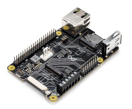
ASX00049

Arduino

* $41.91 - * $50.86

IN STOCK 2867
Buy

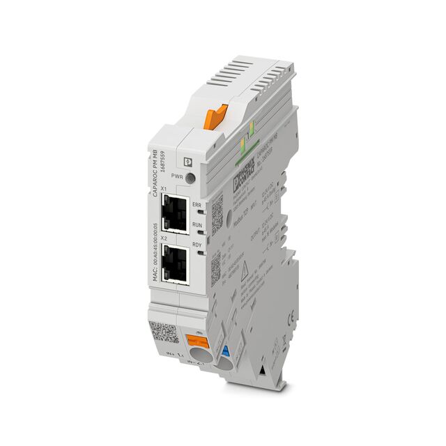
1687559

Phoenix Contact Ltd

[no prices available]

IN STOCK 2
Buy

Reference Designs

RD006

Wurth Elektronik

RD006 - 3 W Dual-output isolated auxiliary supply for communication interfaces and measurement systems

CN0583

Analog Devices Inc.

Multistandard Micropower Verified Smoke Detection System-on-Module

Technical Resources

EVALUATION KITS

EVAL-AD7124-8SDZ

Analog Devices Inc.

$0.00 - * $82.49

IN STOCK 792
Buy
View All